Aluminum Antimonide Sputtering Target Description
Aluminum Antimonide Sputtering Targets are specialized materials used in the sputtering process for the deposition of thin films. Aluminum antimonide is a semiconductor material frequently employed in the development of compound semiconductors. These sputtering targets are utilized to create thin films for various applications, including semiconductor devices, infrared detectors, and other electronic or optoelectronic components.
The Aluminum Antimonide Sputtering Targets provided by TFM are of exceptionally high purity, ensuring stable physical and chemical properties. This high purity guarantees excellent electrical and optical characteristics, making them suitable for both scientific research and production environments with stringent material requirements.
Related Product: Aluminum Nitride Sputtering Target, Aluminum Telluride Sputtering Target
Aluminum Antimonide Sputtering Target Specifications
| Compound Formula | AlSb |
| Molecular Weight | 148.73 |
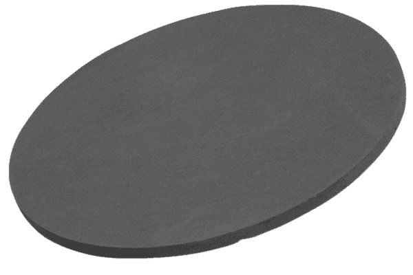
| Appearance | Black Target |
| Melting Point | 1,060℃ |
| Density | 4.26 |
| Available Sizes | Dia.: 1.0″, 2.0″, 3.0″, 4.0″, 5.0″, 6.0″ Thick: 0.125″, 0.250″ |
Aluminum Antimonide Sputtering Target Handling Notes
Indium bonding is recommended for Aluminum Antimonide Sputtering Targets due to their inherent characteristics, such as brittleness and low thermal conductivity, which can make them challenging to handle during sputtering processes. The material’s low thermal conductivity and susceptibility to thermal shock necessitate careful bonding techniques to ensure stable and effective sputtering operations.
Aluminum Antimonide Sputtering Target Application
- Semiconductor Devices: Aluminum antimonide (AlSb) thin films, deposited using sputtering targets, are used in the fabrication of various semiconductor devices, making them suitable for electronic and optoelectronic components.
- Infrared Detectors: AlSb’s performance in the infrared spectrum makes it ideal for use in infrared detectors, sensors, and imaging devices.
- Thermoelectric Devices: AlSb thin films are utilized in thermoelectric devices, where they contribute to energy harvesting and cooling applications.
- Optoelectronic Devices: The semiconductor properties of AlSb make it appropriate for optoelectronic devices, including light-emitting diodes (LEDs) and photodetectors.
Aluminum Antimonide Sputtering Target Packaging
Our Aluminum Antimonide Sputtering Target is meticulously handled during storage and transportation to maintain the quality and integrity of our products.


Reviews
There are no reviews yet.