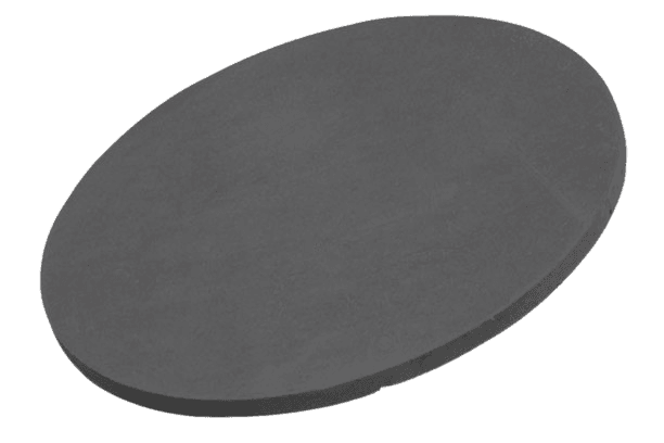
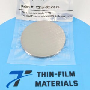
Aluminum Selenide Sputtering Target Description
Aluminum Selenide Sputtering Targets, known for their high purity and fine particle size, are ideal for use in semiconductor and optical instruments, offering a wide range of application possibilities. These targets allow for the deposition of ultra-high purity thin films on solid substrates through sputtering techniques. This process involves ion bombardment, which transforms the target material into a gaseous or plasma phase, enabling precise control over the film deposition.
Aluminum selenide itself is a semiconductor material with unique electrical properties, sitting between a conductor and an insulator. It exhibits high electrical resistivity but demonstrates a photoconductive effect, where its conductivity increases when exposed to light. This makes Aluminum Selenide Sputtering Targets particularly valuable in semiconductor and optical applications, where their ability to respond to light is crucial.
Related Product: Aluminum Nitride Sputtering Target, Aluminum Telluride Sputtering Target
Aluminum Selenide Sputtering Target Specifications
| Compound Formula | Al2Se3 |
| Molecular Weight | 290.84 |
| Appearance | Gray Target |
| Melting Point | – |
| Density | 3.43 g/cm3 |
| Available Sizes | Dia.: 1.0″, 2.0″, 3.0″, 4.0″, 5.0″, 6.0″ Thick: 0.125″, 0.250″ |
Aluminum Selenide Sputtering Target Handling Notes
Indium bonding is advised for the Aluminum Selenide Sputtering Target due to the material’s specific characteristics that can pose challenges during sputtering. Aluminum selenide is brittle and has low thermal conductivity, making it vulnerable to thermal shock. Indium bonding helps mitigate these issues, enhancing the target’s stability and performance throughout the sputtering process.
Aluminum Selenide Sputtering Target Application
Aluminum Selenide Sputtering Targets offer significant advantages in specialized fields such as photovoltaics, optoelectronics, and magnetic materials. With electrical properties that bridge the gap between conductors and insulators, and a photoconductive response that enhances conductivity under light exposure, they are an excellent material choice for these applications. Furthermore, these targets are utilized in chemical vapor deposition (CVD) and physical vapor deposition (PVD) processes, particularly in the development of advanced display technologies, where their unique characteristics contribute to improved performance and efficiency.
Aluminum Selenide Sputtering Target Packaging
Our Aluminum Selenide Sputtering Target is meticulously handled during storage and transportation to ensure that the product maintains its original quality and integrity. We take every precaution to preserve its condition, ensuring that it arrives ready for optimal performance in your applications.


Reviews
There are no reviews yet.