Generic selectors
Exact matches only
Search in title
Search in content
Post Type Selectors

ST0937 Cobalt Silicide Sputtering Target, CoSi2

Chemical FormulaCoSi2
Catalog No.ST0937
CAS Number12017-12-8
Purity99.9%, 99.95%, 99.99%, 99.995%, 99.999%
ShapeDiscs, Plates, Column Targets, Step Targets, Custom-made

Cobalt Silicide sputtering target  come in various forms, purities, sizes, and prices. Thin Film Materials (TFM) manufactures and supplies top-quality sputtering targets at competitive prices.

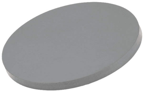
Cobalt Silicide Sputtering Target Description

The Cobalt Silicide Sputtering Target is a crucial material in the sputtering process for creating thin films used in semiconductor and microelectronics manufacturing. This process involves bombarding the target material with high-energy ions, causing atoms or molecules to be ejected and deposited onto a substrate, forming a thin film. Cobalt Silicide, available in various stoichiometries, is highly valued in semiconductor fabrication for its excellent properties.

Thin films are applied to substrates that have been meticulously cleaned and are similar in composition to the target material. By carefully adjusting the sputtering power and rate, along with subsequent processing, films are produced that exhibit excellent electrical conductivity, thermal stability, and minimal stress.

TFM offers Cobalt Silicide Sputtering Targets that ensure high purity, uniform composition, and top-notch film quality. Cobalt Silicide (CoSi2) is particularly noted for its low resistivity and thermal stability, making it a popular choice for contacts in large-scale integrated circuits.

Related Product: Cobalt Oxide Sputtering Targets, Cobalt Sputtering Target

Cobalt Silicide Sputtering Target Specifications

Compound FormulaCoSi2
Molecular Weight115.10
AppearanceBlack Target
Melting Point
Density4.9 g/cm3
Available SizesDia.: 1.0″, 2.0″, 3.0″, 4.0″, 5.0″, 6.0″

Thick: 0.125″, 0.250″

Cobalt Silicide Sputtering Target Handling Notes

Indium bonding is advised for Cobalt Silicide Sputtering Targets because certain characteristics, such as brittleness and low thermal conductivity, make them challenging to sputter effectively. This material is prone to thermal shock due to its low thermal conductivity, so indium bonding helps mitigate these issues, ensuring better performance and stability during the sputtering process.

Cobalt Silicide Sputtering Target Application

Cobalt Silicide Sputtering Targets are versatile materials used across various applications, including Chemical Vapor Deposition (CVD), Physical Vapor Deposition (PVD), and optical processes. Due to its low resistivity and excellent thermal stability, cobalt silicide has become a widely preferred material for contacts in large-scale integrated circuits. Additionally, these sputtering targets hold significant research value and potential applications in the electrical field, making them a valuable choice for both industrial and research purposes.

Cobalt Silicide Sputtering Target Packaging

Our Cobalt Silicide Sputtering Target is meticulously handled during storage and transportation to ensure that the products maintain their original quality and integrity. This careful management guarantees that you receive the sputtering targets in perfect condition, ready for optimal performance in your applications.

Get Contact

TFM offers Cobalt Silicide Sputtering Targets in various forms, purities, sizes, and prices. We specialize in high-purity thin film deposition materials with optimal density and minimal grain sizes, which are ideal for semiconductor, CVD, and PVD applications in display and optics. Contact Us for current pricing on sputtering targets and other deposition materials that are not listed.

Reviews

There are no reviews yet.

Be the first to review “ST0937 Cobalt Silicide Sputtering Target, CoSi2”

Your email address will not be published. Required fields are marked *

Related Products

FAQ

It’s the source material (in solid form) used in sputter deposition to eject atoms or molecules that then form a thin film on a substrate.

Targets can be pure metals (e.g., gold, copper, aluminum), ceramics (e.g., Al₂O₃, SiO₂, TiO₂), alloys, or composites—chosen based on the film’s desired properties.


They are produced by processes such as melting/casting for metals or sintering (often with hot isostatic pressing) for ceramics and composite targets to ensure high density and purity.


In a vacuum chamber, a plasma (typically argon) bombards the target, ejecting atoms that travel and condense on a substrate, forming a thin film.


Key factors include the target’s purity, density, grain structure, and the sputtering yield (i.e. how many atoms are ejected per incident ion), as well as operating conditions like power density and gas pressure.


Operators monitor target erosion (often by measuring the depth of the eroded “race track”) or track total energy delivered (kilowatt-hours) until it reaches a threshold that can compromise film quality.


Fragile materials (such as many ceramics or certain oxides) and precious metals often require a backing plate to improve cooling, mechanical stability, and to allow thinner targets that reduce material costs.


DC sputtering is used for conductive targets, while RF sputtering is necessary for insulating targets (like many oxides) because it prevents charge buildup on the target’s surface.


In reactive sputtering, a reactive gas (e.g., oxygen or nitrogen) is introduced to form compound films on the substrate, but it may also “poison” the target surface if not carefully controlled.


Many manufacturers prefer to control raw material quality by sourcing their own powders; using external powders can risk impurities and inconsistent target properties.


Targets should be stored in clean, dry conditions (often in original packaging or re-wrapped in protective materials) and handled with gloves to avoid contamination, ensuring optimal performance during deposition.

Deposition rate depends on factors such as target material and composition, power density, working gas pressure, substrate distance, and the configuration of the sputtering system (e.g., magnetron design).

 
Shopping Cart
Scroll to Top