Generic selectors
Exact matches only
Search in title
Search in content
Post Type Selectors

ST0963 Gallium Antimonide Sputtering Target, GaSb

Chemical FormulaGaSb
Catalog No.ST0963
CAS Number12064-03-8
Purity99.9%, 99.95%, 99.99%, 99.995%, 99.999%
ShapeDiscs, Plates, Column Targets, Step Targets, Custom-made

Gallium Antimonide sputtering target  come in various forms, purities, sizes, and prices. Thin Film Materials (TFM) manufactures and supplies top-quality sputtering targets at competitive prices.

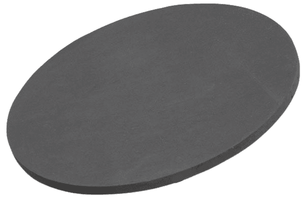
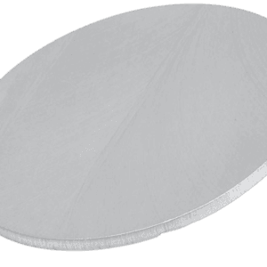
Gallium Antimonide Sputtering Target Description

Gallium Antimonide Sputtering Target is a specialized material designed for use in the sputtering process to deposit thin films. During sputtering, high-energy ions bombard the target, causing atoms to be ejected from the target’s surface. These ejected atoms then deposit onto a substrate, creating a thin film with specific properties.

Gallium Antimonide (GaSb) is a highly versatile semiconductor with tunable conductivity that adapts across different temperature ranges. This makes it ideal for the precise fabrication of electronic components. GaSb features exceptional optical properties with a bandgap of about 0.72 electron volts (eV), making it particularly valuable for developing advanced infrared optics and detectors where precision and sensitivity are crucial.

In addition to its electronic and optical benefits, Gallium Antimonide exhibits stable thermal properties over a wide temperature range. This stability ensures that GaSb performs reliably in high-temperature environments, making it a preferred material for various demanding applications.

Related Product: Gallium (III) Selenide Sputtering Target, CIGS Copper Indium Gallium Antimonide Sputtering Target

Gallium Antimonide Sputtering Target Specifications

Compound FormulaGaSb
Molecular Weight191.48
AppearanceGray Target
Melting Point
Density5.62 g/cm3
Available SizesDia.: 1.0″, 2.0″, 3.0″, 4.0″, 5.0″, 6.0″

Thick: 0.125″, 0.250″

Gallium Antimonide Sputtering Target Handling Notes

For Gallium Antimonide Sputtering Targets, indium bonding is recommended due to the material’s inherent properties that may complicate the sputtering process. Gallium Antimonide can be brittle and has low thermal conductivity, making it prone to thermal shock. Indium bonding helps mitigate these issues, ensuring a more stable and effective sputtering process.

Gallium Antimonide Sputtering Target Application

Infrared Optics: Gallium Antimonide is a key material in the fabrication of infrared optical devices. Its exceptional optical properties, particularly in the infrared spectrum, make it ideal for manufacturing infrared sensors, detectors, and lasers.

Electronics: In the electronics sector, Gallium Antimonide is utilized for its semiconductor capabilities. It is employed in a variety of components, including field effect transistors (FETs), photodiodes, and LEDs, thanks to its adjustable conductivity and reliable performance.

High-Temperature Applications: The material’s stable thermal properties ensure consistent performance across a range of temperatures. This makes Gallium Antimonide suitable for use in high-temperature environments, including aerospace and energy applications.

Semiconductor Technology: Gallium Antimonide’s semiconductor properties are integral to the development of advanced integrated circuits and other semiconductor devices, supporting cutting-edge technology in the field.

Gallium Antimonide Sputtering Target Packaging

Our Gallium Antimonide Sputtering Target is meticulously handled during storage and transportation to ensure that it arrives in optimal condition, maintaining the highest standards of quality.

Get Contact

TFM offers Gallium Antimonide Sputtering Targets in various forms, purities, sizes, and prices. We specialize in high-purity thin film deposition materials with optimal density and minimal grain sizes, which are ideal for semiconductor, CVD, and PVD applications in display and optics. Contact Us for current pricing on sputtering targets and other deposition materials that are not listed.

Reviews

There are no reviews yet.

Be the first to review “ST0963 Gallium Antimonide Sputtering Target, GaSb”

Your email address will not be published. Required fields are marked *

Related Products

FAQ

It’s the source material (in solid form) used in sputter deposition to eject atoms or molecules that then form a thin film on a substrate.

Targets can be pure metals (e.g., gold, copper, aluminum), ceramics (e.g., Al₂O₃, SiO₂, TiO₂), alloys, or composites—chosen based on the film’s desired properties.


They are produced by processes such as melting/casting for metals or sintering (often with hot isostatic pressing) for ceramics and composite targets to ensure high density and purity.


In a vacuum chamber, a plasma (typically argon) bombards the target, ejecting atoms that travel and condense on a substrate, forming a thin film.


Key factors include the target’s purity, density, grain structure, and the sputtering yield (i.e. how many atoms are ejected per incident ion), as well as operating conditions like power density and gas pressure.


Operators monitor target erosion (often by measuring the depth of the eroded “race track”) or track total energy delivered (kilowatt-hours) until it reaches a threshold that can compromise film quality.


Fragile materials (such as many ceramics or certain oxides) and precious metals often require a backing plate to improve cooling, mechanical stability, and to allow thinner targets that reduce material costs.


DC sputtering is used for conductive targets, while RF sputtering is necessary for insulating targets (like many oxides) because it prevents charge buildup on the target’s surface.


In reactive sputtering, a reactive gas (e.g., oxygen or nitrogen) is introduced to form compound films on the substrate, but it may also “poison” the target surface if not carefully controlled.


Many manufacturers prefer to control raw material quality by sourcing their own powders; using external powders can risk impurities and inconsistent target properties.


Targets should be stored in clean, dry conditions (often in original packaging or re-wrapped in protective materials) and handled with gloves to avoid contamination, ensuring optimal performance during deposition.

Deposition rate depends on factors such as target material and composition, power density, working gas pressure, substrate distance, and the configuration of the sputtering system (e.g., magnetron design).

 
Shopping Cart
Scroll to Top