Gallium Phosphide Sputtering Target Description
Gallium Phosphide Sputtering Target is a specialized material designed for the sputtering process used in thin film deposition. During sputtering, high-energy ions bombard the target, causing atoms to be ejected from its surface. These atoms then deposit onto a substrate, forming a thin film with desired properties.
Gallium Phosphide is characterized by its cubic crystal structure, where gallium and phosphorus atoms are arranged in a regular lattice. It has notable optical properties, including a band gap of approximately 2.26 electron volts (eV), making it well-suited for applications in optoelectronics and the manufacturing of optical devices. As a semiconductor, Gallium Phosphide features tunable electrical conductivity, which is advantageous for both electronics and optoelectronic applications.
Although Gallium Phosphide itself is not magnetic, introducing magnetic impurities through specific doping can enable studies in magnetic materials. At room temperature, it behaves as a semiconductor, with its conductivity lying between that of a conductor and an insulator, depending on impurity levels and types. Additionally, Gallium Phosphide demonstrates good thermal stability, making it suitable for high-temperature applications across various environments.
Related Product: Gallium (III) Selenide Sputtering Target, CIGS Copper Indium Gallium Phosphide Sputtering Target
Gallium Phosphide Sputtering Target Specifications
| Compound Formula | GaP |
| Molecular Weight | 100.70 |
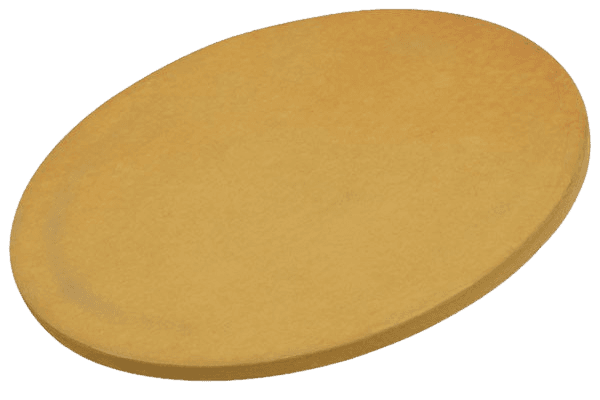
| Appearance | Yellow Target |
| Melting Point | – |
| Density | 4.14 g/cm3 |
| Available Sizes | Dia.: 1.0″, 2.0″, 3.0″, 4.0″, 5.0″, 6.0″ Thick: 0.125″, 0.250″ |
Gallium Phosphide Sputtering Target Handling Notes
Indium bonding is recommended for Gallium Phosphide Sputtering Targets due to the material’s characteristics that can complicate the sputtering process. Gallium Phosphide, with its low thermal conductivity and susceptibility to thermal shock, can present challenges during sputtering. Indium bonding helps mitigate these issues by enhancing thermal management and improving the overall stability of the sputtering process.
Gallium Phosphide Sputtering Target Application
- Optoelectronics: Gallium Phosphide is integral in fabricating optoelectronic devices like LEDs and lasers. Its superior optical characteristics ensure reliability and performance in these applications.
- Semiconductor Devices: As a semiconductor material, Gallium Phosphide is used in creating various semiconductor devices, including field-effect transistors (FETs) and photodetectors. Its electrical properties are crucial for the functionality of these devices.
- Optical Coatings: Gallium Phosphide’s excellent optical attributes make it suitable for preparing high-quality optical coatings. This includes applications in reflector sheets and optical sensors used in lasers and other optical equipment.
- Magnetic Materials Research: When doped with specific elements, Gallium Phosphide is used in research to explore magnetic properties. This can be relevant for developing magnetic storage solutions and sensors.
- Electronic Components: The semiconducting nature of Gallium Phosphide supports the production of various electronic components, including integrated circuits and other essential electronic devices.
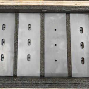
Gallium Phosphide Sputtering Target Packaging
Our Gallium Phosphide Sputtering Target is meticulously managed throughout storage and transportation to maintain its quality and integrity. We ensure that it remains in optimal condition, preserving its performance characteristics for your needs.


Reviews
There are no reviews yet.