Introduction
Gold Palladium (Au/Pd) Sputtering Targets are premium noble metal alloy targets widely used in thin film deposition processes where excellent electrical conductivity, chemical stability, and fine surface morphology are required. By combining gold’s superior conductivity with palladium’s hardness and structural refinement, Au/Pd targets deliver high-performance coatings for precision applications such as electron microscopy, microelectronics, and sensor technologies.
Detailed Description
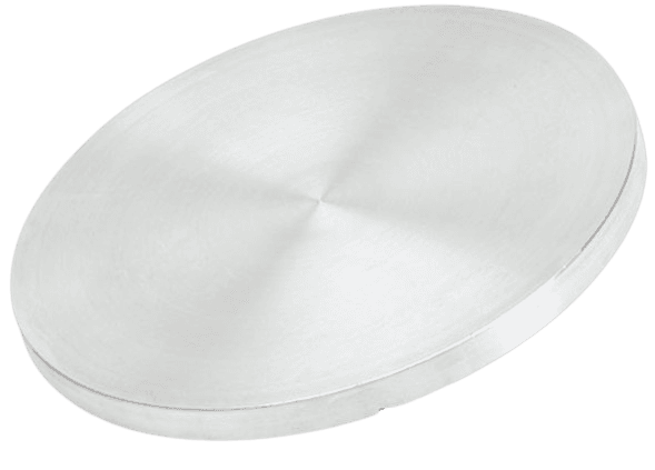
Gold Palladium Sputtering Targets are produced using high-purity raw materials through vacuum induction melting or powder metallurgy routes, ensuring excellent compositional uniformity and structural integrity. The alloy ratio can be precisely controlled—commonly Au:Pd = 60:40 or 80:20 (wt%)—to tailor film characteristics such as grain size, hardness, and conductivity.
One of the key advantages of Au/Pd over pure gold is its refined microstructure. Palladium acts to reduce grain size during deposition, resulting in smoother, more uniform coatings. This is particularly critical in scanning electron microscopy (SEM), where fine-grained conductive coatings minimize charging effects and enhance imaging resolution.
Au/Pd films exhibit excellent adhesion to a wide range of substrates, including polymers, glass, and ceramics. Additionally, the alloy offers improved mechanical durability and wear resistance compared to pure gold, while maintaining strong resistance to oxidation and corrosion.
Targets are available in planar and rotatable forms, and are typically bonded to copper backing plates using indium or elastomer bonding to enhance thermal conductivity and ensure stable sputtering under high power conditions. A dense, fine-grained microstructure (≥99% theoretical density) is essential for minimizing particle generation and ensuring consistent film deposition.
Applications
Gold Palladium Sputtering Targets are widely used in:
- Conductive coatings for SEM and electron microscopy sample preparation
- Thin film circuits and microelectronic devices
- Biosensors and chemical sensor coatings
- Optical coatings and reflective layers
- Decorative coatings with enhanced durability
- Corrosion-resistant conductive films
Technical Parameters
| Parameter | Typical Value / Range | Importance |
|---|---|---|
| Composition | Au/Pd (e.g., 60/40, 80/20 wt%) | Controls film conductivity and morphology |
| Purity | ≥ 99.95% | Ensures high film quality and low contamination |
| Density | ≥ 99% theoretical | Improves sputtering stability and lifetime |
| Diameter | 25 – 200 mm (custom available) | Fits standard sputtering systems |
| Thickness | 2 – 6 mm | Affects deposition rate and target life |
| Bonding | Cu backing / Indium bonding | Enhances heat dissipation and stability |
| Grain Structure | Fine and homogeneous | Ensures smooth, defect-free coatings |
Comparison with Related Materials
| Material | Key Advantage | Typical Application |
|---|---|---|
| Gold Palladium (Au/Pd) | Fine grain, durable, stable films | SEM coatings, sensors |
| Gold (Au) | Highest conductivity | Microelectronics, bonding layers |
| Palladium (Pd) | Higher hardness, catalytic activity | Sensors, catalytic coatings |
FAQ
| Question | Answer |
|---|---|
| Can Au/Pd sputtering targets be customized? | Yes, composition ratio, dimensions, and bonding methods can all be tailored. |
| Why is Au/Pd preferred for SEM coatings? | It produces ultra-fine grain films that reduce charging and improve imaging clarity. |
| What sputtering method is suitable? | DC magnetron sputtering is commonly used due to the metallic nature of the alloy. |
| Are bonded targets necessary? | For high-power or precision applications, bonded targets are recommended for better heat management. |
| What industries use Au/Pd targets most? | Electronics, microscopy, sensor development, and advanced research laboratories. |
Packaging
Our Gold Palladium Sputtering Target are meticulously tagged and labeled externally to ensure efficient identification and maintain high standards of quality control. We take great care to prevent any potential damage during storage and transportation, ensuring the targets arrive in perfect condition.
Conclusion
Gold Palladium Sputtering Targets offer a superior combination of conductivity, surface smoothness, and durability, making them ideal for precision thin film deposition. With flexible composition options and reliable manufacturing quality, Au/Pd targets are a trusted choice for both industrial production and advanced R&D applications.
For detailed specifications and a quotation, please contact us at sales@thinfilmmaterials.com.

Reviews
There are no reviews yet.