
Introduction
Nickel Tungsten (Ni/W) Sputtering Targets are advanced alloy materials widely used in thin film deposition where a balance of mechanical strength, corrosion resistance, and electrical performance is required. By combining the ductility and conductivity of nickel with the hardness and high-temperature stability of tungsten, Ni/W targets enable the deposition of durable, functional coatings for demanding industrial and electronic applications.
Detailed Description
Nickel Tungsten Sputtering Targets are typically produced through powder metallurgy or vacuum melting processes to ensure homogeneous composition and high density. The Ni/W ratio can be tailored (commonly ranging from Ni-rich to W-rich compositions) depending on the desired film properties, such as hardness, conductivity, or resistance to oxidation.
The addition of tungsten significantly enhances the wear resistance, thermal stability, and mechanical strength of nickel-based films. At the same time, nickel improves the overall ductility and sputtering efficiency, allowing for more stable deposition compared to pure tungsten targets.
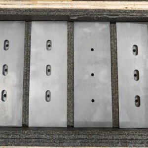
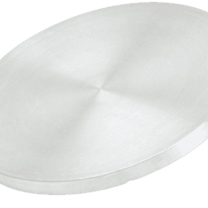
These targets are available in planar or rotatable forms and are often bonded to copper backing plates using indium or elastomer bonding to improve heat dissipation during sputtering. A dense, fine-grained microstructure is essential for minimizing arcing and particle generation, ensuring consistent film thickness and surface quality.
Ni/W coatings are particularly valued for their resistance to corrosion and erosion, as well as their ability to maintain performance under high-temperature or chemically aggressive environments.
Applications
Nickel Tungsten Sputtering Targets are widely used in:
- Corrosion-resistant coatings for harsh environments
- Wear-resistant and hard coatings for mechanical components
- Semiconductor and microelectronic thin films
- Barrier layers and diffusion-resistant coatings
- Decorative coatings with enhanced durability
- Energy systems and functional coatings
Technical Parameters
| Parameter | Typical Value / Range | Importance |
|---|---|---|
| Composition | Ni/W (e.g., 80/20, 70/30 wt%) | Determines film properties |
| Purity | 99.9% – 99.99% | Ensures consistent deposition |
| Density | ≥ 98% theoretical | Improves sputtering stability |
| Diameter | 50 – 300 mm (custom available) | Compatible with sputtering systems |
| Thickness | 3 – 6 mm | Affects target lifetime |
| Bonding | Copper backing / Indium bonding | Enhances thermal conductivity |
| Microstructure | Fine, homogeneous | Reduces defects and arcing |
Comparison with Related Materials
| Material | Key Advantage | Typical Application |
|---|---|---|
| Nickel Tungsten (Ni/W) | Balanced hardness and corrosion resistance | Functional and protective coatings |
| Nickel (Ni) | High conductivity, ductility | Conductive layers |
| Tungsten (W) | Extreme hardness, high melting point | High-temperature coatings |
FAQ
| Question | Answer |
|---|---|
| Can Ni/W sputtering targets be customized? | Yes, composition ratios, size, and bonding options can be tailored to your requirements. |
| What sputtering method is suitable for Ni/W? | Both DC and RF magnetron sputtering can be used depending on system configuration. |
| What is the advantage of alloying Ni with W? | It improves hardness, wear resistance, and thermal stability while maintaining good sputtering performance. |
| Are bonded targets necessary? | For high-power applications, bonded targets improve heat dissipation and structural stability. |
| Which industries use Ni/W targets most? | Semiconductor, energy, aerospace, and advanced coating industries. |
Packaging
Our Nickel Tungsten Sputtering Targets are meticulously tagged and labeled externally to ensure efficient identification and maintain high standards of quality control. We take great care to prevent any potential damage during storage and transportation, ensuring the targets arrive in perfect condition.
Conclusion
Nickel Tungsten Sputtering Targets offer a versatile solution for high-performance thin film deposition, combining the strengths of both nickel and tungsten. With customizable compositions and reliable manufacturing quality, they are ideal for demanding industrial and research applications.
For detailed specifications and a quotation, please contact us at sales@thinfilmmaterials.com.

Reviews
There are no reviews yet.