Barium Zirconium Yttrium Oxide Sputtering Target Description
Barium Zirconium Yttrium Oxide Sputtering Target is notable for its distinctive material properties, particularly its unique crystal structure. This structure provides exceptional qualities essential for semiconductor applications and ensures precision in thin film deposition. Designed for excellence in electronic device manufacturing, this target delivers reliable performance in both research and industrial settings. Its engineered properties make it a superior choice for achieving high-quality thin film coatings and advancing technology.
Related Product: Barium Titanate Sputtering Target, Barium Zirconate Sputtering Target
Barium Zirconium Yttrium Oxide Sputtering Target Specifications
| Compound Formula | BaZrxYyO3 |
| Molecular Weight | – |
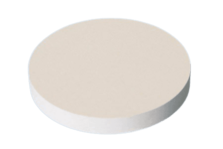
| Appearance | White Target |
| Melting Point | – |
| Density | – |
| Available Sizes | Dia.: 1.0″, 2.0″, 3.0″, 4.0″, 5.0″, 6.0″ Thick: 0.125″, 0.250″ |
Barium Zirconium Yttrium Oxide Sputtering Target Handling Notes
Indium bonding is recommended for Barium Zirconium Yttrium Oxide Sputtering Targets due to the material’s brittleness and low thermal conductivity. These characteristics make it less suitable for direct sputtering applications. The low thermal conductivity and susceptibility to thermal shock further necessitate the use of indium bonding to ensure stable performance and integrity during the sputtering process.
Barium Zirconium Yttrium Oxide Sputtering Target Application
- Electronic Device Preparation: Barium Zirconium Yttrium Oxide Sputtering Targets enhance the performance of electronic devices through precise thin film deposition, leveraging their distinctive crystal structure and electrical characteristics.
- Optoelectronics: The unique crystal structure of Barium Zirconium Yttrium Oxide is crucial in optoelectronics, facilitating the production of photodiodes, lasers, and other optical components with advanced properties.
- Catalytic Applications: The multi-element composition of Barium Zirconium Yttrium Oxide may induce catalytic activity, making it useful in chemical synthesis and energy conversion processes.
- Magnetic Materials Research: The potential magnetic properties of Barium Zirconium Yttrium Oxide contribute to research in magnetic materials, with applications in magnetic memory devices and related studies.
- High-Temperature Stable Materials: Its inherent high thermal stability, due to its crystal structure and elemental composition, makes Barium Zirconium Yttrium Oxide suitable for crafting materials in high-temperature environments.
Barium Zirconium Yttrium Oxide Sputtering Target Packaging
Our Barium Zirconium Yttrium Oxide Sputtering Target is carefully handled during storage and transportation to ensure that the product maintains its quality and integrity.

Reviews
There are no reviews yet.