
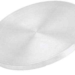
Titanium Silicide Sputtering Target Description
Titanium Silicide (TiSi₂) Sputtering Targets are vital materials for thin film deposition, commonly employed in semiconductor, optical, and electronics industries. TFM proudly presents a comprehensive range of Titanium Silicide Sputtering Targets, designed to meet your exacting specifications and enable precise thin-film coatings with exceptional performance.
Related Product: Titanium Sputtering Target.
Titanium Silicide Sputtering Target Specifications
| Material | Titanium Silicide (TiSi2) |
|---|---|
| Purity | 99.9% and above |
| Shape | Discs, Plates, Custom Shapes, or as per your specifications |
| Size | Dia.: 2.0″, 3.0″, 4.0″, 5.0″, 6.0″ Thick: 0.125″, 0.250″ |
| Sputtering Target Bonding Options | Indium, Elastomer, or Customized |
| Surface Roughness | As machined or as required |
| Melting Point | Approximately 1,650°C |
| Available Documents | Certificate of Analysis (COA), Material Safety Data Sheet (MSDS), and Customized Documents |
We also offer other customized shapes and sizes of the sputtering targets; please Contact Us for more information.
Titanium Silicide Sputtering Target Applications
Our Titanium Silicide Sputtering Targets are suitable for a wide range of applications, including:
- Semiconductor Fabrication: Utilized in the production of semiconductor devices, ensuring precise and reliable thin film coatings.
- Optical Coatings: Essential for optical components, lenses, and mirrors in the optics industry.
- Electronics: Key for electronic circuitry and microelectronics.
- Scientific Research: Employed for thin film deposition in research and development projects.
Packing
Our Titanium Silicide Sputtering Targets are tagged and labeled externally to ensure efficient identification and quality control. We take great care to avoid any damage during storage and transportation, preserving the quality of our products.


Reviews
There are no reviews yet.