Introduction
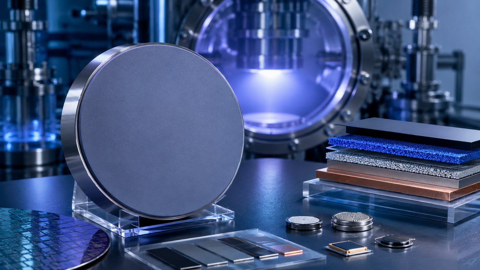
Sputter targets play a pivotal role in thin-film deposition, an essential process used in a wide array of industries. These targets are materials, often metals, alloys, ceramics, or composites, that serve as the source from which atoms are ejected and deposited onto a substrate. The process is part of physical vapor deposition (PVD), which is crucial in producing coatings for everything from semiconductors to solar cells. Understanding the function, material composition, manufacturing techniques, and applications of sputter targets provides a deeper insight into their importance in modern technology and industrial practices.
The Process of Sputtering and the Role of Sputter Targets
At the heart of sputtering is the sputter target, which is exposed to a plasma field in a vacuum chamber. The plasma, typically generated by inert gases like argon, is energized by an electric field, causing atoms in the target material to be ejected. These atoms travel through the chamber and deposit themselves onto a substrate, forming a thin film. This process is highly versatile, allowing for precise control over the thickness, uniformity, and composition of the deposited material.
The sputter target material is a critical factor in determining the properties of the thin film. For example, metal targets such as copper or gold produce conductive films, while ceramic targets such as silicon dioxide provide insulating layers. By altering the target material, one can manipulate the properties of the film to meet the needs of various applications, making sputtering a powerful tool in industries such as electronics, optics, and materials science.
Types of Sputter Targets and Their Materials
Sputter targets come in a variety of materials, each chosen based on the specific requirements of the thin film being created. Metals, alloys, ceramics, and even compounds can serve as sputter targets, and each material imparts different characteristics to the resulting film.
Metal Targets
Metal sputter targets are widely used in applications requiring conductive properties. Metals like gold, silver, copper, aluminum, and platinum are commonly used in the creation of thin films for electronics, optical coatings, and decorative finishes. For instance, gold is often used for coatings in high-performance electronics, while aluminum is chosen for its reflective properties in optical devices.
Alloy Targets
Alloys are another class of sputter targets that combine two or more metals to provide a combination of desirable properties. For example, stainless steel and brass are used for their strength, corrosion resistance, and durability. Alloys can be customized to meet specific needs in industries where a single metal would not provide the necessary performance.
Ceramic Targets
Ceramic sputter targets are typically used when insulation or heat resistance is required. Materials like alumina (Al₂O₃), zirconia (ZrO₂), and silicon dioxide (SiO₂) are common choices in semiconductor and optical industries. Ceramic targets are particularly valuable when creating dielectric layers or coatings for electronic devices, as they help insulate conductive layers and prevent interference.
Compound Targets
Compound sputter targets, such as indium tin oxide (ITO) and tantalum nitride (TaN), are made from materials that combine two or more elements. These targets are especially useful in advanced technologies, such as thin-film solar cells and touchscreen displays. ITO, for example, is widely used for its transparent conductive properties in electronics, while TaN is used in the creation of thin films for protective coatings in high-temperature applications.
Magnetic Targets
Magnetic sputter targets are used in applications requiring magnetic properties. Materials like iron, cobalt, and nickel are commonly used to create films that are used in data storage devices, magnetic sensors, and actuators. Magnetic sputtering helps create films with controlled magnetic properties, which is critical in devices like hard drives, which rely on the manipulation of magnetic fields for data storage.
The Manufacturing Process of Sputter Targets

Creating high-quality sputter targets involves specialized production methods that ensure purity, uniformity, and the right structural properties. The manufacturing process varies depending on the target material, but generally includes techniques such as casting, sintering, and pressing.
For metal sputter targets, a common method is casting, where metal is melted in a furnace and poured into molds. Once solidified, the target is machined to the required shape. This process is used for metals like copper and aluminum, which are relatively easy to cast.
Ceramic and compound targets, however, require different approaches. Powder metallurgy is often used for these materials, involving the compaction of fine powders under high pressure and temperature to create a dense, uniform target. The resulting target is then sintered to remove any porosity and enhance its density. This ensures that the sputter target performs efficiently during the deposition process.
Cold isostatic pressing (CIP) and hot isostatic pressing (HIP) are additional methods used to improve the quality of the target. CIP involves applying high pressure to the powder material, ensuring even density across the entire target. HIP, on the other hand, combines both high temperature and pressure to eliminate any remaining voids in the material, resulting in a highly dense and durable sputter target.
In some cases, vacuum induction melting (VIM) is used for producing high-purity metal targets, especially for reactive or high-melting-point metals. This method involves melting the material under a vacuum to prevent contamination, ensuring the target’s purity.
Key Properties of Sputter Targets
The performance of sputter targets is defined by a range of properties that determine their suitability for different applications. Some of the most important properties include purity, density, grain size, and thermal and electrical conductivity.
Purity
One of the most critical properties for sputter targets, particularly in semiconductor and high-tech industries, is purity. Impurities in the target material can affect the quality of the thin film and compromise the performance of the devices being produced. To meet the stringent requirements of these industries, sputter targets are often manufactured to extremely high levels of purity, sometimes exceeding 99.99%.
Density
The density of a sputter target impacts its sputtering efficiency and the uniformity of the deposited film. High-density targets are preferred because they release more atoms with each plasma interaction, leading to a more efficient sputtering process. Denser targets also produce films that are smoother and more uniform.
Grain Size
The grain size of a sputter target affects the quality of the thin film. A smaller grain size generally results in a smoother film with fewer defects. In addition, a fine grain structure can improve the target’s resistance to cracking and degradation during the sputtering process, leading to a longer-lasting target.
Thermal and Electrical Conductivity
Thermal conductivity is an important factor in determining the efficiency of the sputtering process. Targets with high thermal conductivity dissipate heat effectively, preventing overheating and ensuring consistent deposition. Electrical conductivity is also relevant, especially for metal targets used in electronics, as conductive films are often required.
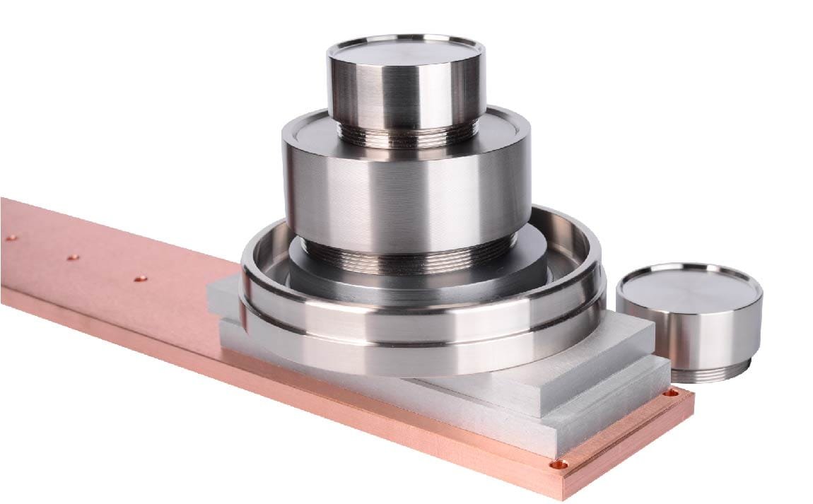
What Size Are Sputtering Targets?
Sputtering targets come in a wide range of sizes, tailored to the needs of different applications and sputtering equipment. Common sizes range from small discs, approximately 1 inch (2.54 cm) in diameter for laboratory or research purposes, to larger targets over 12 inches (30 cm) in diameter used in industrial-scale production. Thickness varies as well, with thinner targets for lower-output applications and thicker ones for high-volume, long-duration sputtering.
Rectangular or planar targets are also widely used, especially for coating large surfaces. The size of the sputter target is carefully chosen based on factors like deposition rate, area of coverage, and equipment specifications to ensure efficient and effective thin film production.
Applications of Sputter Targets in Various Industries
Sputter targets are used in a wide range of industries, owing to their versatility in producing thin films with tailored properties. Some of the key sectors that rely on sputter targets include electronics, optics, solar energy, and data storage.
In the electronics industry, sputter targets are used to create the conductive films that form the interconnections in semiconductor devices. These films are crucial in microelectronics, where thin and precise layers are required to ensure optimal device performance. Metal targets like copper, gold, and aluminum are commonly used in this sector.
In optics, sputter targets are employed to create thin films for optical coatings, including reflective coatings for mirrors and antireflection coatings for lenses. These coatings improve the functionality and efficiency of optical devices, such as telescopes, microscopes, and camera lenses. For example, titanium or aluminum targets are frequently used in these applications.
Sputter targets are also integral to the solar energy industry, where materials like indium tin oxide (ITO) and cadmium telluride (CdTe) are used to create thin-film solar cells. These materials help enhance the light absorption and electrical efficiency of solar panels, making them more effective in converting sunlight into electricity.
In the data storage industry, magnetic sputter targets are used to create thin magnetic films for hard disk drives (HDDs) and other storage devices. These films are crucial for storing data, as they must be magnetically stable and capable of holding information over long periods.
Conclusion
Sputter targets are essential to the process of sputtering, which is at the heart of thin-film deposition technology. They allow for the precise deposition of a wide range of materials onto substrates, creating thin films that are critical to modern technology. From electronics and optics to solar cells and data storage, sputter targets are used in many industries to produce films with specific properties that enhance the performance and functionality of devices. The ongoing development of sputter target materials and manufacturing processes will continue to drive advancements in technology, enabling the creation of new and more efficient devices across various sectors.