Generic selectors
Exact matches only
Search in title
Search in content
Post Type Selectors

Ceramic Sputtering Targets

Oxide Ceramic Sputtering Targets

Oxide ceramic sputtering targets are commonly used for their high melting points, excellent insulation, and resistance to oxidation and corrosion. These targets are made by sintering simple or complex oxides and are ideal for applications in electronics, optics, and energy devices.

Common Oxide Ceramic Targets

We offer various oxide ceramic targets including:

  • Al₂O₃ (Aluminum Oxide)
  • SiO₂ (Silicon Dioxide)
  • Nb₂O₅ (Niobium Oxide)
  • TiO₂ (Titanium Dioxide)
  • ITO (Indium Tin Oxide)
  • AZO (Aluminum-doped Zinc Oxide)
  • YSZ (Yttria-stabilized Zirconia)
  • IGZO (Indium Gallium Zinc Oxide)

Key Features

Our oxide ceramic targets feature smooth surfaces, uniform color, and no cracks or contaminants. They are heat-resistant and durable, making them suitable for long-term use.

Customization & Bonding

We provide round (1″ to 14″ diameter) and rectangular targets, and can customize sizes as needed. These targets are bonded with copper backing plates using indium or elastomer to enhance durability.

For custom orders or more details, contact us at sales@thinfilmmaterials.com or call (786) 825-8645.

Ceramic Sputtering Targets (Planar Type)

Material Name Chemical Formula Purity Action
Aluminum Nitride AlN 99.50%
Aluminum Oxide Al2O3 99.99%
Antimony Oxide Sb2O3 99.99%
Antimony Selenide Sb2Se3 100.00%
Antimony Sulfide Sb2S3 99.99%
Antimony Telluride Sb2Te3 100.00%
AZO Al2O3/ZnO 2/98 wt% 99.99%
Barium Carbonate BaCO3 99.90%
Barium Cerium Yttrium Zirconate BaCe(1-x-y)Y(x)Zr(y)O3 99.90%
Barium Ferrite BaFe12O19 99.90%
Barium Fluoride BaF2 99.90%
Barium Oxide BaO 99.90%
Barium Strontium Titanate Ba(1-x)Sr(x)TiO3 99.90%
Barium Strontium Titanate Ba0.5Sr0.5TiO3 99.90%
Barium Titanate BaTiO3 99.90%
Barium Zirconate BaZrO3 99.90%
Bismuth Antimony Telluride Bi0.5Sb1.5Te3 99.99%
Bismuth Calcium Ferrite Bi0.9Ca0.1FeO3 99.90%
Bismuth Dysprosium Iron Gallate Bi2DyFe4GaO12 99.90%
Bismuth Ferrite BiFeO3 99.90%
Bismuth Ferrite (Garnet) Bi3Fe5O12 99.90%
Bismuth Lanthanum Ferrite Bi(1-x) LaxFeO3 99.90%
Bismuth Lutetium Iron Gallate Bi1.5Lu1.5Fe4GaO12 99.90%
Bismuth Manganate Bi2.4MnO3 99.90%
Bismuth Oxide Bi2O3 99.99%
Bismuth Selenide Bi2Se3 99.99%
Bismuth Telluride Bi2Te3 100.00%
Bismuth Titanate Bi4Ti3O3 99.99%
Boron Carbide B4C 99.50%
Boron Nitride BN 99.50%
Boron Oxide B2O3 99.90%
Cadmium Oxide CdO 99.9% - 99.99%
Cadmium Selenide CdSe 100.00%
Cadmium Stannate Cd2SnO4 99.9% - 99.99%
Cadmium Sulfide CdS 99.99%
Cadmium Telluride CdTe 99.99%
Calcium Fluoride CaF2 99.90%
Calcium Oxide CaO 99.95%
Calcium Phosphate Ca3(PO4)2 99.90%
Calcium Phosphate Tribasic Ca10 (OH)2 (PO4)6 99.90%
Calcium Titanate CaTiO3 99.99%
Cerium Bismuth Ferrite Ce2.2Bi0.8Fe5O12 99.99%
Cerium Fluoride CeF3 99.90%
Cerium Hexaboride Sputtering Target CeB6 99.50%
Cerium Oxide CeO2 99.90%
Cerium Yttrium Ferrite Ce2.5Y0.5Fe5O12 99.90%
Chromium Nitride CrN 99.50%
Chromium Oxide Cr2O3 99.90%
Chromium Oxide CrO3 99.90%
Chromium Silicate CrSiO2 99.90%
Chromium Silicide CrSi 99.50%
Chromium Silicide CrSi2 99.50%
Cobalt Ferrite CoFe2O4 99.90%
Cobalt Oxide Co3O4 99.90%
Cobalt Oxide CoO 99.90%
Copper Aluminum Oxide CuAlO2 99.90%
Copper Oxide Cu2O 99.90%
Copper Oxide CuO 99.90%
Copper Selenide Cu2Se 99.99%
Copper Sulfide Cu2S 99.99%
Copper Sulfide CuS 99.99%
Copper Telluride Cu2Te 99.99%
Cupper Indium Gallium Selenide CIGS 99.99%
Dysprosium Oxide Dy2O3 99.90%
Erbium Oxide Er2O3 99.90%
Europium Nickel Oxide EuNiO3 99.90%
Europium Oxide Eu2O3 99.50%
Europium Titanate EuTiO3 99.90%
Gadolinium Cerium Oxide Gd0.2Ce0.8O2 99.90%
Gadolinium Oxide Gd2O3 99.90%
Gallium Oxide Ga2O3 99.9% - 99.99%
Germanium Antimony Telluride Ge2Sb2Te5 99.99%
Germanium Oxide GeO2 99.9% - 99.99%
Germanium Telluride GeTe 100.00%
Germanium Telluride GeTe4 99.99%
Hafnium Boride HfB2 99.50%
Hafnium Carbide HfC 99.50%
Hafnium Nitride HfN 99.50%
Hafnium Oxide HfO2 99.99%
Hafnium Telluride HfTe 99.99%
Holmium Oxide Ho2O3 99.9% - 99.95%
Indium Aluminum Zinc Oxide In2O3/Al2O3/ZnO 65/16/19 wt% 99.99%
Indium Gallium Zinc Oxide (IGZO) InGaZnO4 99.99%
Indium Iron Oxide InFe2O4 99.90%
Indium Molybdenum Oxide In2O3/Mo 98/2 wt% 99.99%
Indium Oxide In2O3 99.99%
Indium Selenide In2Se3 99.99%
Indium Selenide InSe 99.99%
Indium Sulfide In2S3 99.99%
Indium Tin Oxide (ITO) ITO, In2O3/SnO2, 90/10 wt% 99.99%
Indium Zinc Oxide (IZO) Sputtering Targets IZO, In2O3/ZnO, 90/10 wt% 99.99%
Iridium Oxide IrO2 99.90%
Iron Boride FeB 99.50%
Iron Oxide Fe2O3 99.5 - 99.9%
Iron Oxide Fe3O4 99.9% - 99.99%
Iron Silicide Fe3Si 99.50%
Lanthanum Aluminate LaAlO3 99.90%
Lanthanum Calcium Manganate La0.5Ca0.5MnO3 99.90%
Lanthanum Calcium Manganate La0.7Ca0.3MnO3 99.90%
Lanthanum Calcium Manganate La1-xCaxMnO3 99.90%
Lanthanum Copper Manganate La2CuMnO6 99.90%
Lanthanum Copper Oxide La2CuO4 99.90%
Lanthanum Ferrite LaFeO3 99.90%
Lanthanum Gallate LaGaO3 99.90%
Lanthanum Hexaboride LaB6 99.50%
Lanthanum Lithium Titanate La(1-x) LixTiO3 99.90%
Lanthanum Manganate LaMnO3 99.90%
Lanthanum Nickel Oxide LaNiO3 99.90%
Lanthanum Oxide La2O3 99.99%
Lanthanum Praseodymium Calcium Manganate La(1-x-y)PrxCayMnO3 99.90%
Lanthanum Scandium Oxide LaScO3 99.90%
Lanthanum Strontium Chromate La(1-x)SrxCrO3 99.90%
Lanthanum Strontium Cobalt Iron Oxide (LSCF)  LaxSr1-xCoyFe1-yO3 99.90%
Lanthanum Strontium Cobalt Oxide La0.5Sr0.5CoO3 99.90%
Lanthanum Strontium Copper Oxide La(1-x)SrxCuO4 99.90%
Lanthanum Strontium Manganate La0.67Sr0.33MnO3 99.90%
Lanthanum Strontium Manganate La0.7Sr0.3MnO3 99.90%
Lanthanum Strontium Manganate La0.9Sr0.1MnO3 99.90%
Lanthanum Strontium Manganate La1-xSrxMnO3 99.90%
Lanthanum Titanate LaTiO3 99.90%
Lanthanum Vanadium Oxide LaVO3 99.90%
Lead Calcium Titanate Pb0.7Ca0.3TiO3 99.90%
Lead Lanthanum Zirconium Titanate (PLZT) Pb1-xLax(ZryTi1-y)1-0.25xO3 99.90%
Lead Oxide PbO 99.90%
Lead Sulfide PbS 99.90%
Lead Telluride PbTe 99.99%
Lead Titanate PbTiO3 99.90%
Lead Zirconate PbZrO3 99.90%
Lead Zirconate Titanate with Niobium PbZr0.52Ti0.48O3 with 1 at% Nb 99.90%
Lead Zirconium Titanate PZT, PbZr0.52Ti0.48O3 99.90%
Lithium Cobalt Oxide LiCoO2 99.99%
Lithium Fluoride LiF 99.90%
Lithium Iron PhosphateSputtering Targets LiFePO4 99.90%
Lithium Manganate LiMn2O4 99.90%
Lithium Nickel Cobalt Oxide LiNi(1-x)CoxO2 99.90%
Lithium Nickel Manganese Cobalt Oxide LiNi0.33Mn0.33Co0.33O2 99.90%
Lithium Nickel Phosphate LiNiPO4 99.99%
Lithium Nickel Vanadium Oxide LiNiVO4 99.90%
Lithium Niobate LiNbO3 99.99%
Lithium Phosphate Li3PO4 99.99%
Lithium Silicate Li4SiO4 99.99%
Lithium Tantalate LiTaO3 99.90%
Lithium Titanate Li4Ti5O12 99.90%
Lithium Zirconate Li6Zr2O7 99.90%
Lutetium Oxide Lu2O3 99.9% - 99.99%
Magnesium aluminate MgAl2O4 99.90%
Magnesium Diboride MgB2 99.50%
Magnesium Fluoride MgF2 99.90%
Magnesium Oxide MgO 99.95%
Magnesium Silicide Mg2Si 99.50%
Magnesium Zinc Oxide Mg(1-x) ZnxO 99.95%
Manganese Cobalt Oxide MnCo2O4 99.90%
Manganese Oxide MnO 99.90%
Manganese Selenide MnSe 99.90%
Manganese Sulfide MnS 99.90%
Manganese Telluride MnTe 99.90%
Molybdenum Carbide Mo2C 99.50%
Molybdenum Disilicide MoSi2 99.50%
Molybdenum Disulfide MoS2 99.99%
Molybdenum Oxide MoO3 99.90%
Molybdenum Selenide MoSe2 99.90%
Molybdenum Telluride MoTe2 99.90%
Neodymium Aluminate NdAlO3 99.90%
Neodymium Copper Oxide Nd2CuO4 99.90%
Neodymium Gadolinium Oxide NdGdO3 99.90%
Neodymium Nickel Oxide NdNiO3 99.90%
Neodymium Oxide Nd2O3 99.90%
Neodymium Strontium Manganate Nd(1-x)SrxMnO3 99.90%
Nickel Ferrite NiFe2O4 99.90%
Nickel Oxide NiO 99.90%
Niobium Carbide NbC 99.50%
Niobium Nitride NbN 99.50%
Niobium Oxide Nb2O5 99.95%
Niobium Oxide Nb2Ox 99.95%
Potassium Fluoride KF 99.90%
Potassium Niobate KNbO3 99.95%
Praseodymium Calcium Manganate Pr0.7Ca0.3MnO3 99.90%
Praseodymium Cerium Manganate Pr(1-x)CexMnO3 99.90%
Praseodymium Nickel Oxide PrNiO 99.90%
Praseodymium Oxide Pr2O3 99.90%
Ruthenium Oxide RuO2 99.90%
Samarium Cerium Copper Oxide Sm(1-x)CexCuO4 99.90%
Samarium Copper Oxide SmCuO4 and Sm2CuOx 99.90%
Samarium Oxide Sm2O3 99.9% - 99.99%
Scandium Oxide Sc2O3 99.9% - 99.99%
Selenium Oxide SeO2 99.90%
Silicon Carbide SiC 99.50%
Silicon Dioxide SiO2 100.00%
Silicon Monoxide SiO 99.90%
Silicon Nitride Si3N4 99.90%
Silver Sulfide Ag2S 99.99%
Silver Telluride Ag2Te 99.99%
Sodium Fluoride NaF 99.90%
Sodium Niobate NaNbO3 99.99%
Strontium Aluminate doped with Europium SrAl2O4 with 3 wt% Eu 99.90%
Strontium Bismuth Niobate SBN (SrBi2Nb2O9) 99.90%
Strontium Bismuth Tantalate SBT (Sr0.8Bi2.2Ta2O9) 99.90%
Strontium Copper Oxide SrCuO2 99.90%
Strontium Lead Oxide Sr3PbO 99.90%
Strontium Manganate SrMnO3 99.90%
Strontium Niobium Titanate SrNb(1-x)TixO3 99.90%
Strontium Oxide SrO 99.50%
Strontium Ruthanate SrRuO3 99.90%
Strontium Titanate SrTiO3 99.90%
Strontium Zirconate SrZrO3 99.90%
Tantalum Carbide TaC 99.50%
Tantalum Nitride TaN 99.50%
Tantalum Oxide Ta2O5 99.95%
Tantalum Oxide Ta2Ox 99.95%
Tantalum Silicide TaSi2 99.50%
Tellurium Oxide TeO2 99.9% - 99.99%
Terbium Ferrite Tb3Fe5O12) 99.90%
Terbium Manganate TbMnO3 99.90%
Terbium Oxide Tb4O7 99.9% - 99.95%
Tin Oxide SnO2 99.99%
Tin Selenide SnSe 99.99%
Tin Sulfide SnS 99.99%
Tin Sulfide SnS2 99.99%
Titanium Boride TiB2 99.50%
Titanium Carbide TiC 99.50%
Titanium Dioxide TiO2 99.99%
Titanium Disilicide TiSi2 99.50%
Titanium Ferrite TiFe2O4 99.90%
Titanium Monoxide TiO 99.90%
Titanium Nitride TiN 99.50%
Tungsten Carbide WC 99.95%
Tungsten Disilicide WSi2 99.50%
Tungsten Disulfide WS2 99.80%
Tungsten Oxide WO3 99.90%
Tungsten Selenide WSe2 99.80%
Tungsten Telluride WTe2 99.80%
Vanadium Carbide VC 99.50%
Vanadium Dioxide VO2 99.90%
Vanadium Oxide V2O5 99.90%
Ytterbium Oxide Yb2O3 99.90%
Yttrium Aluminum Oxide Y3Al5O12 99.90%
Yttrium Ferrite Y3Fe5O12 99.90%
Yttrium Manganate YMnO3 99.90%
Yttrium Oxide Y2O3 99.90%
Zinc Oxide ZnO 99.9, 99.99%
Zinc Oxide Alumina  (AZO) ZnO/Al2O3 (2% Standard Doping) 99.99%
Zinc Oxide doped with Gallium Oxide (GZO) GZO, ZnO/Ga2O3 95/05 wt% 99.99%
Zinc Oxide doped with Magnesium Zn0.9Mg0.1O 99.90%
Zinc Oxide doped with Manganese ZnO with 0.3 wt% Mn 99.90%
Zinc Oxide doped with Manganese ZnO with 4 wt% Mn 99.90%
Zinc Oxide doped with Scandia ZnO/Sc2O3 98/02 wt% 99.90%
Zinc Oxide doped with Sodium Zn0.99Na0.01O 99.90%
Zinc Selenide ZnSe 99.90%
Zinc Sulfide ZnS 99.99%
Zinc Telluride ZnTe 99.99%
Zirconia Fully Stabilized with Yttria (YSZ) ZrO2 (fully stabilized - Y2O3) 99.90%
Zirconia stabilized with Yttria Zr(1-x)YxO2 99.90%
Zirconium Boride ZrB2 99.50%
Zirconium Carbide ZrC 99.50%
Zirconium Nitride ZrN 99.50%
Zirconium Oxide ZrO2 99.90%
Zirconium Telluride ZrTe 99.99%

Understanding Ceramic Sputtering Targets: A Comprehensive Overview

With innovations continuously driving the need for more efficient and reliable coating techniques, ceramic sputtering targets have emerged as a significant material choice. Their unique properties—such as high thermal stability, excellent chemical resistance, and desirable electrical characteristics—make them indispensable in creating thin films with precise control over thickness, composition, and structure. In the following sections, we will address frequently asked questions and key topics that potential users, researchers, and industry professionals often search for online.

Table of Contents

Chapter 1

What Are Ceramic Sputtering Targets?

Ceramic Sputtering Targets are engineered ceramic materials specifically designed for use in sputtering deposition processes. Sputtering is a method where energetic particles, typically ions, bombard a target material causing atoms or molecules to be ejected and subsequently deposited onto a substrate. In the context of ceramic sputtering targets, these materials often comprise oxides, nitrides, carbides, or other ceramic compounds that have been processed to achieve high density and uniformity.

The primary attributes that define these targets include their purity, homogeneity, and stability under plasma conditions. Due to their ceramic nature, these targets offer excellent resistance to thermal shock and chemical degradation. They can be tailored to exhibit properties such as high dielectric strength, low thermal conductivity, and robust mechanical integrity—qualities that are critical in various applications from semiconductor manufacturing to optical coatings.

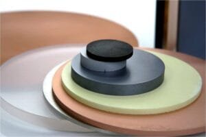
Moreover, ceramic sputtering targets are available in different forms and sizes to suit specific sputtering systems and deposition requirements. They can be manufactured using advanced powder metallurgy techniques, including high-temperature sintering and hot isostatic pressing, ensuring that the target material exhibits a fine-grained microstructure and minimal porosity. This high degree of densification is essential to maintain consistent sputtering yields and to avoid particulate contamination during the deposition process.

Chapter 2

How Are Ceramic Sputtering Targets Manufactured?

The production of ceramic sputtering targets is a highly controlled process involving several sophisticated techniques aimed at achieving optimal density and purity. The manufacturing process typically starts with high-purity ceramic powders, which are mixed with binders and other additives to achieve a homogeneous mixture. This mixture is then compacted into the desired shape through processes such as isostatic pressing or uniaxial pressing.

Following compaction, the green body (the pressed compact) is subjected to a sintering process. Sintering involves heating the material to a temperature below its melting point to facilitate atomic diffusion and bonding between particles. In many cases, pressure-assisted sintering techniques, like hot pressing or hot isostatic pressing, are used to achieve higher densification and reduce the presence of residual porosity. The goal is to produce a target that has a uniform microstructure and is free from cracks or defects that could compromise its performance during sputtering.

Quality control is critical at every stage of production. Advanced characterization techniques, such as scanning electron microscopy (SEM), X-ray diffraction (XRD), and density measurements, are employed to ensure that the ceramic sputtering targets meet stringent specifications. These techniques verify not only the purity and phase composition of the ceramic but also its grain size distribution and overall homogeneity.

Additionally, the final targets are often subjected to post-sintering treatments, including grinding and polishing, to achieve the precise dimensions and surface finish required for efficient sputtering. The combination of precise manufacturing techniques and rigorous quality control helps ensure that ceramic sputtering targets deliver consistent performance and reliability in demanding industrial applications.

Chapter 3

What Materials Are Used in Ceramic Sputtering Targets?

Ceramic sputtering targets are composed of a variety of ceramic compounds, each chosen for its unique properties and suitability for specific applications. Some of the most commonly used materials include:

  • Metal Oxides: Materials such as indium tin oxide (ITO), zinc oxide (ZnO), and titanium dioxide (TiO₂) are widely used in optoelectronic applications due to their transparency and electrical conductivity. ITO, in particular, is popular in the display and photovoltaic industries.
  • Nitrides: Silicon nitride (Si₃N₄)and aluminum nitride (AlN) are employed in high-temperature and high-power electronic applications because of their excellent thermal conductivity and electrical insulation properties.
  • Mixed Ceramic Compounds: In some cases, ceramic sputtering targets are engineered by combining different ceramic materials to tailor their properties. This can include blending oxides with nitrides or carbides to achieve a balance of conductivity, transparency, and mechanical strength.

The choice of material is dictated by the requirements of the deposition process and the final application of the thin film. For instance, in the semiconductor industry, the purity and stoichiometry of the ceramic target are critical, whereas in decorative coatings, the optical properties might be of greater importance. Advances in material science have enabled the development of composite and doped ceramic targets that offer enhanced performance characteristics, such as improved sputtering rates and better adhesion properties.

Chapter 4

What Are the Key Advantages of Ceramic Sputtering Targets?

Ceramic sputtering targets offer several advantages over their metallic counterparts and other deposition materials. Their inherent properties translate into performance benefits that are highly valued in various industrial and research applications:

  • Thermal Stability: One of the most significant advantages of ceramic materials is their ability to withstand high temperatures. This property ensures that ceramic sputtering targets can operate efficiently even under the high-energy conditions of sputtering processes without degrading.
  • Chemical Inertness: Ceramics are resistant to chemical reactions, which minimizes the risk of contamination during deposition. This quality is particularly important in semiconductor manufacturing, where purity is paramount.
  • Electrical Properties: Many ceramic materials can be engineered to exhibit specific electrical characteristics, such as high dielectric strength or controlled conductivity. This is beneficial for applications requiring precise electronic properties in the thin films.
  • Wear Resistance: Ceramic targets are less prone to erosion compared to metallic targets. Their hardness and low sputtering yield contribute to a longer operational lifetime and more consistent film deposition.
  • Environmental Stability: Ceramics are resistant to corrosion and oxidation, which is advantageous in harsh environments or in processes that involve reactive gases.
  • Customizability: The ability to tailor ceramic compositions through doping or by creating composite materials allows for the optimization of target properties for specific applications.

These advantages make ceramic sputtering targets highly desirable for producing high-quality, uniform thin films that meet the rigorous demands of modern technological applications. Whether in the production of advanced electronic devices, energy-efficient coatings, or optical components, the benefits of ceramic targets contribute significantly to improved performance and reliability.

Chapter 5

How Do Ceramic Sputtering Targets Compare to Metal Sputtering Targets?

A common question among industry professionals is how ceramic sputtering targets differ from metal sputtering targets. Both types of targets are used in sputtering deposition, but they offer distinct advantages and are chosen based on the application requirements.

  • Material Properties: Metal targets are generally prized for their high electrical conductivity and ease of sputtering, making them suitable for applications where metallic films are desired. In contrast, ceramic targets often provide better thermal stability, chemical resistance, and tailored electrical properties, which are essential for semiconductor and optical applications.
  • Sputtering Efficiency: Metal targets usually have higher sputtering yields due to their lower binding energies, which can lead to faster deposition rates. However, ceramic targets, with their denser structure, can offer more uniform deposition with less particulate generation, which is crucial for applications requiring high film quality.
  • Film Characteristics: The films produced from metal targets are typically metallic in nature, which may require additional processing to achieve the desired electrical or optical properties. Ceramic targets, on the other hand, allow for the direct deposition of dielectric, semiconducting, or insulating films, reducing the need for post-deposition modifications.
  • Operational Lifespan: Ceramic targets often exhibit longer lifespans under high-energy plasma conditions, thanks to their superior hardness and resistance to erosion. This makes them more cost-effective in long-term, high-volume production environments.
  • Cost Considerations: While ceramic sputtering targets might be more expensive to produce due to their complex manufacturing processes and high material purity requirements, their extended service life and performance benefits can justify the initial investment.

Ultimately, the choice between ceramic and metal sputtering targets depends on the specific requirements of the deposition process and the intended application of the thin film. For industries that demand precision, durability, and high performance—such as semiconductor manufacturing, advanced optics, and renewable energy—ceramic targets offer a compelling advantage.

Chapter 6

What Are the Common Applications of Ceramic Sputtering Targets?

Ceramic sputtering targets are integral to a wide array of applications across diverse industries. Their versatility and superior properties have enabled breakthroughs in several high-tech fields:

  • Semiconductor Manufacturing: In the semiconductor industry, ceramic sputtering targets are used to deposit dielectric films, barrier layers, and insulating coatings on silicon wafers. Materials like silicon nitride (Si₃N₄) and titanium dioxide (TiO₂) are common in these processes, contributing to the performance and reliability of microelectronic devices.
  • Display Technology:  
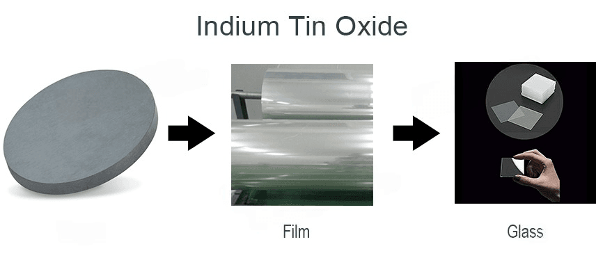
Transparent conductive oxides, such as indium tin oxide (ITO), are deposited from ceramic targets to produce films for flat-panel displays, touch screens, and photovoltaic cells. These films combine high electrical conductivity with optical transparency, critical for modern display technology.
  • Optics and Photonics: Ceramic sputtering targets are employed in the fabrication of anti-reflective coatings, optical filters, and laser components. The ability to deposit thin films with controlled refractive indices and high durability is essential for the performance of optical devices.
  • Energy Applications: In the renewable energy sector, ceramic sputtering targets are used to create thin-film coatings for solar cells. Oxide and nitride films can improve the efficiency and longevity of photovoltaic devices by enhancing light absorption and reducing reflective losses.
  • Protective Coatings: Beyond electronic and optical applications, ceramic sputtering targets are also used for depositing hard, wear-resistant coatings on industrial components. These coatings improve the durability and performance of tools, cutting instruments, and other mechanical parts exposed to harsh operating conditions.

The diversity of applications is a testament to the flexibility and robustness of ceramic sputtering targets. By selecting the appropriate ceramic composition and optimizing the sputtering parameters, manufacturers can achieve highly specific film characteristics tailored to meet the demands of cutting-edge technologies.

Chapter 7

What Are the Quality Control Measures in Ceramic Sputtering Target Production?

Given the critical role that ceramic sputtering targets play in high-tech applications, ensuring their quality is paramount. Manufacturers implement rigorous quality control protocols throughout the production process to guarantee that each target meets strict industry standards. Key quality control measures include:

  • Material Purity Verification: The production process begins with high-purity powders. Analytical techniques such as inductively coupled plasma (ICP) spectroscopy are used to verify the elemental composition and detect any impurities that could affect performance.
  • Microstructural Analysis: Techniques like scanning electron microscopy (SEM) and X-ray diffraction (XRD) are employed to analyze the microstructure and phase composition of the sintered ceramic. This ensures that the grain size distribution is uniform and that the target is free from undesired phases or defects.
  • Density and Porosity Testing: Achieving high density is essential for sputtering targets. Manufacturers use methods such as Archimedes’ principle and helium pycnometry to measure the density and porosity of the targets, ensuring they meet the required specifications.
  • Dimensional Accuracy and Surface Quality: Post-sintering processes such as grinding and polishing are followed by precise dimensional inspections to confirm that the targets conform to the required size and surface finish. Any deviation can lead to uneven sputtering and poor film quality.
  • Performance Testing: Finally, the targets are subjected to actual sputtering tests under controlled conditions. This practical evaluation confirms that the target will perform reliably in industrial sputtering systems, delivering the desired deposition rate and film uniformity.

These quality control measures are vital to maintaining the high standards demanded by industries such as semiconductor manufacturing and advanced optics. By adhering to stringent testing protocols, manufacturers ensure that each ceramic sputtering target contributes to the overall performance and reliability of the thin-film deposition process.

Chapter 8

What Are the Challenges and Limitations of Ceramic Sputtering Targets?

Despite their many advantages, ceramic sputtering targets also present certain challenges and limitations that must be addressed during both production and application:

  • Manufacturing Complexity: The production of high-quality ceramic sputtering targets involves complex sintering and densification processes. Achieving a defect-free microstructure requires precise control over temperature, pressure, and material composition. Any deviations in these parameters can result in targets with inconsistent performance.
  • Cost Considerations: Due to the sophisticated manufacturing processes and high-purity materials required, ceramic sputtering targets tend to be more expensive than their metal counterparts. For some applications, the higher initial cost can be a barrier, despite the long-term benefits of improved durability and performance.
  • Sputtering Efficiency: While ceramics offer excellent film quality, their sputtering yields are generally lower than those of metals. This means that the deposition rates can be slower, which may impact production efficiency in high-volume manufacturing settings.
  • Material-Specific Limitations: The performance of a ceramic sputtering target is highly dependent on its composition. Some ceramic materials might be more susceptible to cracking or delamination under prolonged high-power sputtering conditions. Moreover, variations in target composition can lead to differences in film properties, requiring careful optimization for each application.
  • Integration with Existing Systems: Not all sputtering systems are optimized for ceramic targets. Adapting existing equipment or developing new configurations to accommodate the specific requirements of ceramic materials can involve additional investment and technical challenges.

Despite these challenges, ongoing research and development in materials science and process engineering continue to address these limitations. Manufacturers are constantly improving the production techniques, optimizing the target compositions, and developing innovative solutions to enhance sputtering efficiency and reduce production costs.

Chapter 9

Where to Buy Ceramic Sputtering Targets and What Are the Pricing Considerations?

thin-film-logo

For companies and research institutions looking to invest in high-quality ceramic sputtering targets, selecting a trusted supplier is essential. The market is specialized, with several manufacturers offering tailored solutions for semiconductor, optics, and renewable energy applications.

  • Supplier Selection: Choosing the right supplier requires careful evaluation of product quality, manufacturing consistency, and the ability to offer customized solutions. TFM is a leading provider in this field, known for its precision-engineered ceramic sputtering targets that meet the highest industry standards.

  • Pricing Considerations: The cost of ceramic sputtering targets depends on factors such as material composition, size, and order volume. Compared to metal targets, ceramic options often involve more complex production processes, contributing to a higher price point. However, TFM’s advanced manufacturing techniques ensure extended target lifespan and superior film quality, delivering long-term value for customers.

  • Customization and Technical Support: TFM offers a wide range of standard and customized sputtering targets to meet specific deposition needs. Additionally, its team of experts provides technical support and consultation services to help optimize sputtering performance and maximize efficiency.

  • Global Availability: With a strong global presence, TFM ensures competitive pricing and reliable international shipping, catering to clients worldwide. Industry exhibitions and trade shows also serve as excellent platforms for learning about the latest advancements in sputtering technology and connecting with leading suppliers like TFM.

By partnering with TFM, customers can secure high-performance ceramic sputtering targets that align with both their technical requirements and budget constraints.

Chapter 10

Future Trends in Ceramic Sputtering Target Technology

The field of ceramic sputtering targets is continually evolving, driven by the increasing demand for advanced thin-film deposition technologies and the rapid pace of innovation in materials science. Several future trends are emerging that promise to shape the next generation of sputtering targets:

  • Advanced Composite Materials: Researchers are exploring novel composite ceramic materials that combine the best properties of different ceramics. By doping or blending ceramics with metals or other compounds, it is possible to enhance sputtering yields, improve film uniformity, and further extend target lifespans.
  • Nanostructured Targets: Innovations in nanotechnology are paving the way for the development of nanostructured ceramic targets. These targets could offer superior control over grain size and surface morphology, leading to ultra-smooth films with enhanced electrical and optical properties.
  • Energy Efficiency Improvements: As industries strive to reduce energy consumption and production costs, advancements in sputtering system design and target manufacturing processes are expected. More energy-efficient sputtering targets that require lower power inputs without compromising performance will be in high demand.
  • Sustainability and Environmental Considerations: With an increasing focus on sustainability, manufacturers are exploring eco-friendly production techniques and materials. Efforts to reduce waste, lower emissions during target production, and utilize recycled materials are gaining momentum in the industry.
  • Integration with Emerging Technologies: The growth of emerging fields such as flexible electronics, wearable devices, and advanced photonics is driving demand for new sputtering target formulations. Ceramic targets specifically engineered for these applications could open new avenues for innovation, offering the precise material properties required for next-generation devices.
  • Digitalization and Process Automation: Advanced monitoring techniques, real-time quality control systems, and process automation are set to further refine the production of ceramic sputtering targets. These developments will not only enhance product quality but also reduce manufacturing variability and improve overall efficiency.

As research continues and technological barriers are overcome, the ceramic sputtering target industry is poised to deliver even more robust, efficient, and versatile materials for a wide range of applications.

Chapter 11

Frequently Asked Questions

Ceramic sputtering targets often provide superior resistance to oxidation, higher hardness, and better stability in high-temperature environments compared to metal targets.

Ceramic sputtering targets are available in various purities, typically ranging from 99% to 99.999% (5N), depending on the application and deposition quality requirements.

Lifespan depends on factors such as target material composition, power settings, deposition rate, sputtering pressure, and uniformity of plasma distribution.

To prevent cracking, manufacturers use high-density processing techniques and uniform bonding methods. Additionally, controlled heating and cooling cycles during sputtering help reduce thermal stress.

Yes, some ceramic targets can be reprocessed or reformed into new targets. Recycling depends on the composition and the level of contamination during use.

Ceramic targets are often bonded using elastomeric bonding, indium bonding, or silver bonding to improve thermal conductivity and reduce mechanical stress.

Yes, due to their ceramic nature, these targets are more brittle than metal targets, making proper handling and mounting essential to prevent damage.

Oxide ceramic targets are commonly used for transparent conductive coatings, while nitride ceramics provide excellent hardness, wear resistance, and chemical stability for applications like hard coatings and semiconductors.

Impurities can cause defects, alter electrical or optical properties, and introduce unwanted contamination into the deposited film, making high-purity targets essential for precise applications.

Ceramic targets such as ITO (Indium Tin Oxide) and ZnO (Zinc Oxide) are widely used for transparent conductive films in LCDs, OLEDs, and touchscreens.

Ceramic sputtering targets are mainly used in physical vapor deposition (PVD) techniques such as magnetron sputtering and RF sputtering.

Ceramic materials typically have lower thermal expansion coefficients than metals, reducing stress-related issues in high-temperature applications. However, some ceramics may require special bonding techniques to accommodate thermal expansion mismatches.

Chapter 12

Conclusion

Ceramic sputtering targets play a crucial role in high-performance thin film manufacturing, finding widespread applications in semiconductors, display technology, optical coatings, and renewable energy. With their exceptional high-temperature resistance, chemical stability, and precision manufacturing, ceramic targets have become indispensable materials across various critical industries.

As materials science and manufacturing technologies continue to advance, the performance and applications of ceramic sputtering targets are also expanding. High-purity, high-density, and finely structured ceramic targets have become key factors in enhancing thin film quality and deposition efficiency, providing reliable support for precision manufacturing. At the same time, the industry’s demand for higher-performance materials is driving the development of new ceramic targets, laying the foundation for future technological innovations.

Whether in semiconductor device fabrication, optical coatings, or emerging energy technologies, ceramic sputtering targets play a vital role in improving thin film performance and optimizing process stability. As market demand grows and technological breakthroughs continue, ceramic targets are poised to unlock even greater potential in advanced applications.

Shopping Cart
Scroll to Top