| Material Type | Strontium Bismuth Tantalate |
| Symbol | SBT (Sr0.8Bi2.2Ta2O9) |
| Color/Appearance | |
| Melting Point (°C) |
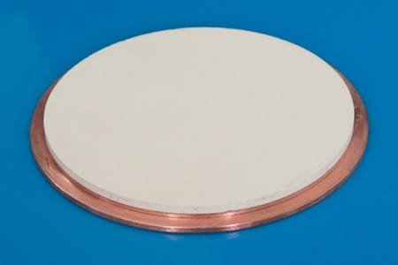
Strontium Bismuth Tantalate Sputtering Targets
TFM offers Strontium Bismuth Tantalate (SrBi₂Ta₂O₉) Sputtering Targets, designed for thin-film deposition applications in advanced industries. These targets are known for their unique ferroelectric and piezoelectric properties, making them ideal for use in memory devices, capacitors, and sensor applications. With their high performance, Strontium Bismuth Tantalate sputtering targets are extensively used in electronic, optical, and energy storage applications.
Key Features and Advantages
High Purity – TFM’s Strontium Bismuth Tantalate sputtering targets are available in 99.9% purity, ensuring the deposition of high-quality films with consistent material properties.
Ferroelectric Properties – Known for their ferroelectric behavior, these targets are commonly used in non-volatile memory, piezoelectric devices, and optical coatings.
Excellent Thin Film Deposition Performance – Provides high-quality thin films used in advanced applications such as ferroelectric memories, multilayer capacitors, and smart sensors.
Customizable Sizes – Available in custom sizes to meet specific application needs, from research to large-scale production.
Stable and Durable – Manufactured using cold pressing and sintering techniques, ensuring high-density targets and reliable performance during deposition.
Specifications
Purity: 99.9%
Target Types Available:
Circular Targets: Diameter ≤ 14 inches, Thickness ≥ 1mm
Block Targets: Length ≤ 32 inches, Width ≤ 12 inches, Thickness ≥ 1mm
Applications
Ferroelectric Memory Devices – Strontium Bismuth Tantalate is used in non-volatile memory devices and random access memory (RAM) due to its ferroelectric properties.
Piezoelectric Devices – Applied in the manufacturing of sensors, actuators, and energy harvesters for automotive, medical, and industrial applications.
Optical Coatings – Used for antireflection coatings, optical filters, and thin-film mirrors in laser and display technologies.
Capacitors – Utilized in multilayer ceramic capacitors (MLCCs) for advanced electronic and telecommunication devices.
Manufacturing Process
Cold Pressing & Sintering – Ensures that the sputtering targets have high density and optimal performance for thin-film deposition.
Elastomer Bonding – The targets are bonded to a backing plate to improve deposition uniformity and handling during sputtering.
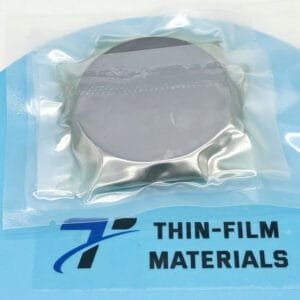
Cleaning & Packaging – Thoroughly cleaned and packaged to avoid contamination and ensure that the targets are ready for use in vacuum environments.
Options
Custom Sizes – Custom dimensions available to meet the specific needs of your application.
R&D Sizes – Smaller sizes are available for research and development, offering flexibility for experimental and prototype work.
Sputtering Target Bonding Service – For improved performance and long-lasting thin films, a target bonding service is available to enhance sputtering efficiency.
Industry Impact
TFM’s Strontium Bismuth Tantalate Sputtering Targets are essential materials for industries requiring high-performance thin films, such as electronics, energy storage, sensor technologies, and optical coatings. With high purity, excellent ferroelectric and piezoelectric properties, and customizable sizes, these targets enable the fabrication of cutting-edge devices in areas such as ferroelectric memories, actuators, capacitors, and optical sensors.


Reviews
There are no reviews yet.