Display and touch-panel thin-film stacks may use transparent conductive oxides such as ITO and IGZO together with metal or oxide layers selected for the required device structure.
When selecting a target, define the material or composition, purity and density basis when required, planar or rotary geometry, target dimensions, backing or bonding configuration, and the cathode model or drawing. Browse the sputtering target catalog for available material paths.
For quotation review, provide the film-stack context, target specifications, quantity, and inspection or documentation requirements through the TFM contact and RFQ path.



Photovoltaic thin-film processes may use sputtering targets and evaporation materials for conductive, absorber, buffer, contact, and transparent-electrode layers. Candidate materials depend on the device architecture and can include silicon, CdTe, CdSe, CdS, CIGS-related compositions, ITO, AZO, copper, indium, gallium, selenium, and tellurium.
Use the sputtering target catalog and evaporation materials catalog to identify the appropriate source form. An RFQ should state the material or composition, purity basis, dimensions or charge form, quantity, deposition source or cathode information, and documentation requirements.
Submit the available process context, drawing, or specification through the TFM contact and RFQ path for quotation review.



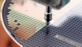
Semiconductor thin-film fabrication can use sputtering targets and evaporation materials for conductive, barrier, adhesion, dielectric, electrode, and other device-stack layers. The source material and configuration must be selected for the specific process module and contamination limits.
Specify the material or composition, purity basis, geometry, dimensions, backing or bonding requirement, deposition source or cathode model, quantity, and inspection or documentation needs. Browse the sputtering target catalog and evaporation materials catalog, then send the process and equipment details through the TFM contact and RFQ path.


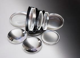
Optical thin-film stacks can be deposited by evaporation, sputtering, or a combination of methods. Material selection depends on the required optical function, wavelength range, substrate, deposition source, and qualification plan.
For source-material review, provide the compound or elemental material, purity basis, target or evaporation form, dimensions or charge size, quantity, and equipment information. Browse sputtering targets and evaporation materials, then submit the coating-stack context and specification through the TFM contact and RFQ path.


LED and optoelectronic thin-film processes may use metal, alloy, oxide, nitride, and transparent-conductive source materials for contacts, electrodes, barriers, reflectors, and other stack functions. Candidate materials can include aluminum, titanium, nickel, silver, gold, platinum, tungsten, tungsten-titanium, and ITO, subject to the device design.
For quotation review, specify the material or composition, purity basis, target or evaporation form, dimensions, quantity, equipment or cathode details, backing or bonding requirement, and documentation needs. Start with the sputtering target catalog or evaporation materials catalog.


Magnetic data-storage stacks can use multiple sputtered metal, alloy, oxide, and compound layers. Candidate source materials may include platinum- and ruthenium-based materials, but the required composition and configuration depend on the media or head process and the intended film stack.
For an RFQ, provide the material or alloy ratio, purity basis, target dimensions, quantity, cathode or drawing information, backing or bonding configuration, and inspection or documentation requirements. Review the sputtering target catalog and submit the stack context through the TFM contact and RFQ path.


Architectural, automotive, display, and electrochromic glass can use multilayer thin-film stacks for optical, electrical, reflective, or thermal functions. Depending on the stack design, source materials may include transparent conductive oxides, metals, alloys, and other oxide compounds.
Selection should be based on the required film stack, substrate size, deposition method, target or evaporation-source form, dimensions, quantity, and equipment interface. Browse sputtering targets and evaporation materials, then provide the drawing, cathode or source details, and documentation requirements through the TFM contact and RFQ path.