Thin Film Displays (TFD) are essential information carriers, found in a variety of applications worldwide. Among these, Liquid Crystal Displays (LCDs) dominate as the most popular panel technology due to their versatility in sizes and configurations. To perform effectively, LCDs and other display types—such as Twisted Nematic (TN), Super Twisted Nematic (STN), Thin Film Transistor LCD (TFT LCD), Organic Light Emitting Diodes (OLED), and Micro-OLED—rely on a transparent conductive oxide (TCO) film. Indium Tin Oxide (ITO) is the industry-standard TCO, but Indium Gallium Zinc Oxide (IGZO) is rapidly gaining traction for its higher mobility characteristics.
TFM stands as a global leader in producing ITO and IGZO targets, ensuring high standards through an in-house manufacturing process. Each production stage is tightly controlled to maintain quality across crucial material properties, including composition, density, purity, and bond coverage, guaranteeing consistency within each batch and across different batches. In addition to ITO, TFM provides an extensive selection of metal targets—such as molybdenum, aluminum, copper, and titanium—tailored for various TFD applications, from LCDs and touch sensors to EMI coatings for notebooks, color-shifting coatings for mobile phones, and hard coatings for wearable devices.
With a dedicated R&D and technical team, TFM also offers comprehensive recycling services for its materials and production waste, supporting sustainable practices throughout the display industry.


TFM Photovoltaics (PV) stands at the forefront of renewable energy as a powerful, inexhaustible source of clean power. In recent years, advancements in sputter target quality and the development of alternative materials have significantly boosted PV technology, driving increased efficiency in solar cells. Among these advancements, Heterojunction Technology (HJT) PV panels have gained considerable traction. This technology combines the high efficiency of crystalline silicon with the benefits of amorphous silicon thin-film, making it one of the most effective solutions for maximizing solar energy output and efficiency.
TFM supplies a wide array of high-quality PVD sputter targets and evaporation materials specifically for solar applications. Essential materials include amorphous silicon (a-Si), CdTe, CdSe, CdTeZn, CdS, and CIGS, along with high-purity Cu, In, Ga, Se, and Te evaporation materials. Each of these materials offers unique optical properties that play a critical role in improving solar cell efficiency. TFM’s knowledgeable sales team is available to discuss the specific benefits of each material and how it can enhance PV performance.
TFM is committed to sustainable production and offers recycling services for all materials and production waste. With the support of an experienced R&D and technical team, TFM helps clients maximize resource efficiency, reduce waste, and advance sustainable practices in solar manufacturing.


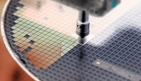
Physical vapor deposition (PVD) sputter targets and evaporation materials play a pivotal role in semiconductor chip fabrication, enhancing both front-end and back-end processes. As the industry moves beyond simple chip densification, the focus has shifted to integrating additional functionality to meet evolving technological demands.
TFM is uniquely positioned to supply PVD sputter targets and evaporation materials, with a strong commitment to sustainable sourcing. Many raw materials are derived through in-house recycling, or “urban mining,” where materials are reclaimed and refined. TFM’s integrated refining, melting, casting, forging, rolling, and bonding processes enable precise control over critical material properties, including purity, grain size, and homogeneity, ensuring optimal performance in PVD applications.
TFM’s comprehensive production resources are bolstered by a dedicated R&D team, available to assist customers with process enhancements. From developing new material compositions and geometries to testing layer stack deposits in TFM’s own applications lab, TFM offers tailored solutions that optimize the PVD process and advance semiconductor technology.


Physical Vapor Deposition (PVD) by evaporation remains a top technology for creating optical thin-film coatings. As demands tighten for optical filter coatings across medical, defense, and commercial applications, there is a notable shift towards sputter deposition with optical monitoring. While sputtering technology gains traction for these precise applications, evaporation will continue to play an essential role in the coating process.
The integration of optical components into semiconductor applications is also on the rise to meet the growing consumer demand for enhanced speed. A prime example is the incorporation of optical components directly on semiconductor chips, known as “Photronics,” a new field of semiconductor technology.
TFM is a leading supplier of PVD evaporation and sputtering materials, sourced through a sustainable process of in-house reclamation or “urban mining.” This sustainable sourcing is complemented by TFM’s comprehensive in-house capabilities, which include refining, melting, casting, forging, rolling, and bonding. These steps allow TFM to maintain precise control over critical material attributes like purity, grain size, and homogeneity, ensuring high-performance outcomes in the PVD process.
TFM’s advanced production capabilities are further supported by a skilled R&D team dedicated to assisting customers with process improvements. This includes developing new material compositions and geometries or applying layer stacks in TFM’s applications lab, enabling tailored solutions for advanced optical coatings and semiconductor integration.


A Light Emitting Diode (LED) is an electroluminescent semiconductor device, widely utilized in home and industrial lighting, outdoor displays, automotive lighting, and mobile applications. As the LED industry matures, manufacturers are focused on enhancing performance and reducing costs, which opens doors to new applications. TFM is strategically positioned to support these advancements in LED technology.
TFM’s in-house recycling and refining services ensure a stable supply of high-quality materials, backed by stringent control over raw materials and sputter target production processes, including Vacuum Induction Melting (VIM), Hot Pressing (HP), and Hot Isostatic Pressing (HIP). This closed-loop recycling system not only maintains high standards but also reduces the overall cost of ownership for customers by repurposing spent targets. Additionally, TFM has introduced a target leasing program for various metals and precious metals. This program allows customers to lease targets based on utilization rates or to receive credits for returned metal values according to daily prices, minus recycling fees.
TFM offers a wide range of standard sputter target and evaporation materials for LED applications, including aluminum (Al), titanium (Ti), nickel (Ni), silver (Ag), gold (Au), platinum (Pt), tungsten (W), tungsten-titanium (WTi), and indium tin oxide (ITO). The selection of materials depends on specific application requirements and processes, enabling customers to achieve optimal performance across diverse LED applications.


Data storage has experienced remarkable growth over the past decade, driven by an insatiable demand for immediate access to information from any location. Devices such as smartphones, tablets, IoT devices, and enterprise solutions are all increasingly connected to the “Cloud,” further enhancing the need for efficient data management.
Hard Disk Drives (HDDs) remain the most cost-effective solution for global data centers. TFM supplies a comprehensive range of sputtering targets, including precious and non-precious metals such as platinum (Pt) alloys, platinum oxides, ruthenium (Ru), ruthenium alloys, ruthenium oxides, and non-precious alloys. These materials are essential for both magnetic disks and heads, enabling high-performance data storage solutions.
TFM’s in-house recycling and refining services ensure a stable supply of materials with consistent quality. By maintaining strict control over raw materials and production processes—including Vacuum Induction Melting (VIM), Hot Pressing (HP), and Hot Isostatic Pressing (HIP)—TFM is uniquely positioned to offer a closed-loop recycling service for spent targets, significantly reducing the overall cost of ownership for customers.
To further enhance value for clients, TFM has implemented a target leasing program for various metals and precious metals. This program is based on target utilization rates and provides credits for returned metal values according to daily prices, minus recycling fees. This innovative approach supports sustainable practices while ensuring customers have access to the materials they need for optimal data storage solutions.