
Chromium Silicide Sputtering Target Description
Our chromium silicide sputtering target is a high-performance ceramic target composed of chromium and silicon. Designed for precision sputtering applications, this target is ideal for thin film deposition processes in semiconductor, display, and other advanced technology industries.
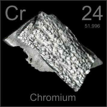
Chromium is a chemical element derived from the Greek word chroma, meaning “color.” It was used as early as 1 AD and was discovered by the Terracotta Army. The canonical chemical symbol for chromium is Cr. Its atomic number is 24, and it is located in Period 4 and Group 6 of the periodic table, belonging to the d-block. The relative atomic mass of chromium is 51.9961(6) Dalton, with the number in brackets indicating the uncertainty.
Related Product: Chromium Sputtering Target
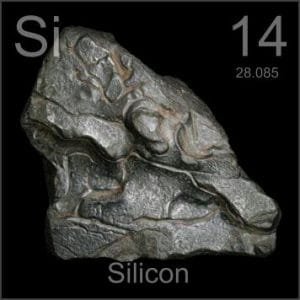
Silicon is a chemical element derived from the Latin words silex or silicis, meaning “flint.” It was first mentioned in 1824 and observed by J. Berzelius, who also accomplished and announced its isolation. The canonical chemical symbol for silicon is Si. Its atomic number is 14, and it is located in Period 3 and Group 14 of the periodic table, belonging to the p-block. The relative atomic mass of silicon is 28.0855(3) Dalton, with the number in brackets indicating the uncertainty.
Chromium Silicide Sputtering Target Handling Notes
- Bonding Recommendation for Chromium Silicide Sputtering TargetIndium bonding is recommended for chromium silicide sputtering targets due to the material’s characteristics that are not ideal for conventional sputtering methods. These characteristics include brittleness and low thermal conductivity, which can affect the target’s performance and longevity.
- Thermal Properties of Chromium Silicide Sputtering TargetChromium silicide sputtering targets have low thermal conductivity and are susceptible to thermal shock. This means they can experience significant stress and potential damage when subjected to rapid temperature changes during sputtering processes.
Chromium Silicide Sputtering Target Application
The chromium silicide sputtering target is utilized in a range of applications, including:
- Thin Film Deposition: For creating thin layers in various electronic and optical devices.
- Decoration: In decorative coatings for aesthetic purposes.
- Semiconductor: Essential in semiconductor fabrication for various components.
- Display: Used in the production of display panels.
- LED and Photovoltaic Devices: Applied in the manufacturing of LEDs and photovoltaic cells.
- Functional Coating: For enhancing the properties of materials with functional coatings.
- Optical Information Storage: In industries focused on optical data storage.
- Glass Coating: For coating automotive glass, architectural glass, and other specialized glass products.
- Optical Communication: In devices and systems used for optical communication.
Chromium Silicide Sputtering Target Packing
Our chromium silicide sputter targets are meticulously tagged and labeled externally to facilitate efficient identification and ensure rigorous quality control. We take great care to prevent any damage during storage and transportation, maintaining the highest standards for product integrity.
Get Contact
TFM offers Chromium Silicide Sputtering Targets in various forms, purities, sizes, and prices. We specialize in high-purity thin film deposition materials with optimal density and minimal grain sizes, which are ideal for semiconductor, CVD, and PVD applications in display and optics. Contact Us for current pricing on sputtering targets and other deposition materials that are not listed.


Reviews
There are no reviews yet.