Introduction
The Molybdenum Disilicide Sputtering Target (MoSi₂) is a high-performance ceramic compound target widely used in thin film deposition for applications requiring excellent thermal stability, oxidation resistance, and electrical conductivity. MoSi₂ is a well-known refractory silicide material that combines the high-temperature durability of molybdenum with the chemical stability of silicon-based compounds.
MoSi₂ thin films deposited through magnetron sputtering or other physical vapor deposition (PVD) techniques are commonly used in semiconductor devices, diffusion barrier layers, high-temperature coatings, and microelectronic components. Its ability to maintain structural integrity and resist oxidation at elevated temperatures makes it particularly valuable for demanding industrial and research applications.
Detailed Description
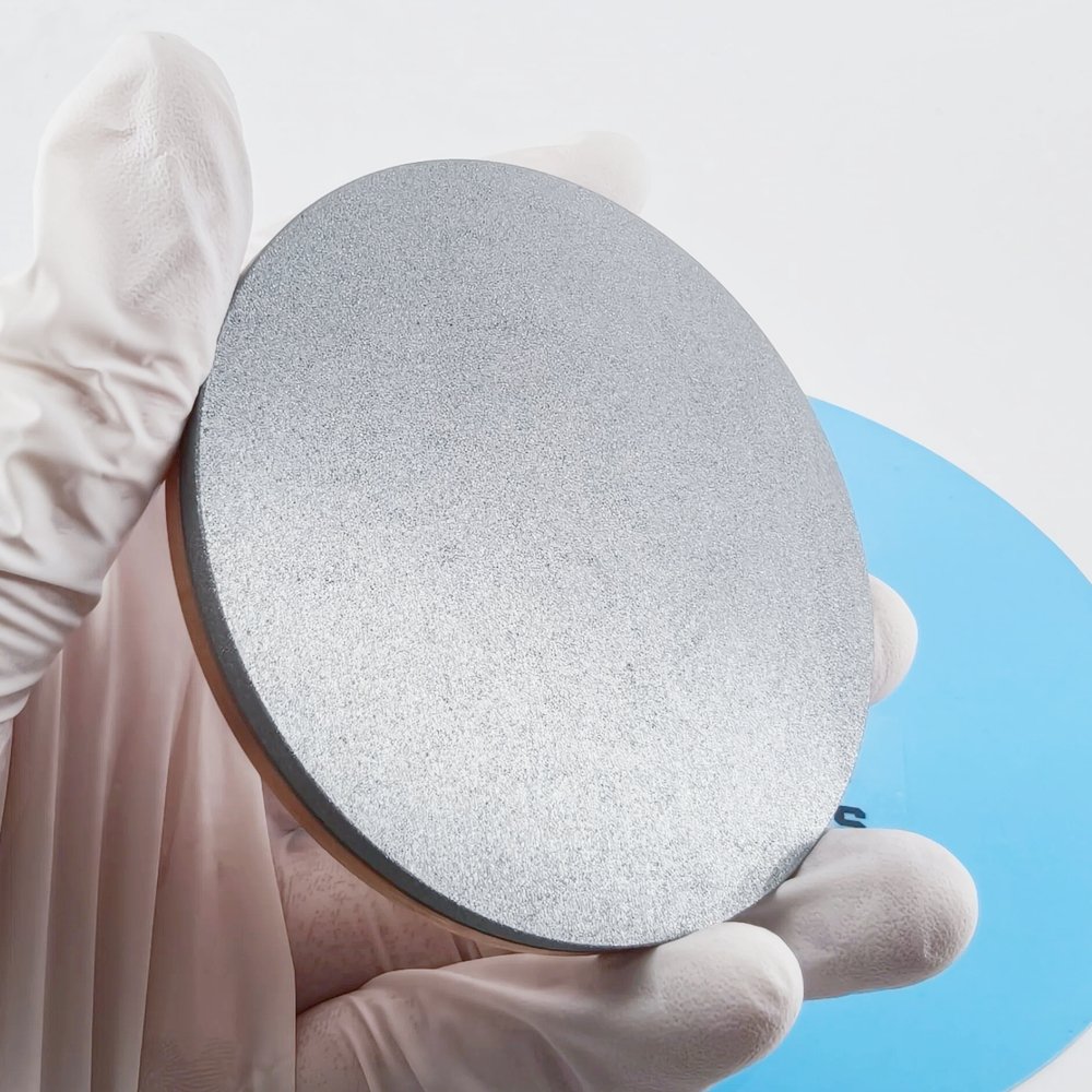
Molybdenum Disilicide sputtering targets are typically manufactured using high-purity molybdenum and silicon through advanced ceramic processing techniques such as hot pressing, vacuum sintering, or hot isostatic pressing (HIP). These processes produce dense, homogeneous targets with controlled stoichiometry, which is essential for stable sputtering performance and uniform thin film deposition.
MoSi₂ is a refractory intermetallic compound with a melting point exceeding 2000 °C and excellent resistance to oxidation at high temperatures. When exposed to oxygen at elevated temperatures, MoSi₂ forms a protective silicon dioxide (SiO₂) layer on its surface, which helps prevent further oxidation and improves long-term durability.
In thin film applications, MoSi₂ coatings provide excellent thermal stability, electrical conductivity, and diffusion barrier performance. These characteristics make MoSi₂ films suitable for microelectronic device structures where stable conductive layers and high-temperature reliability are required.
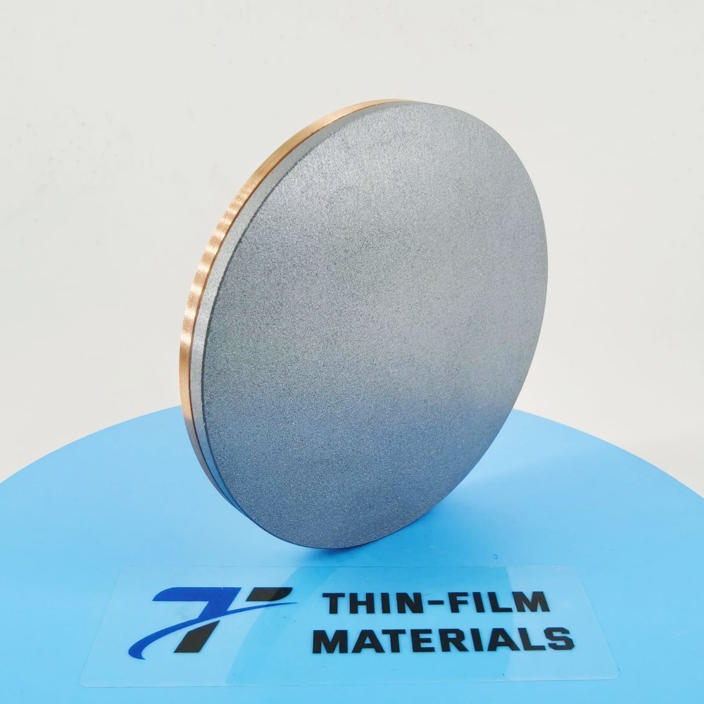
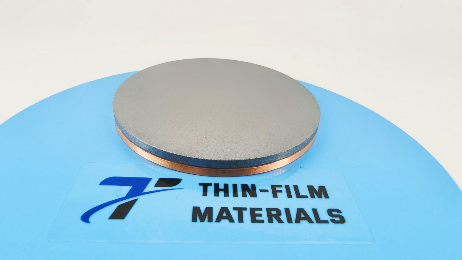
High-density MoSi₂ sputtering targets help ensure stable sputtering rates, reduced particle generation, and improved film uniformity. For high-power sputtering systems, MoSi₂ targets can be supplied as bonded targets with copper backing plates, typically using indium bonding or diffusion bonding techniques to improve heat transfer and mechanical stability during operation.
Applications
Molybdenum Disilicide sputtering targets are widely used in several advanced technology sectors:
Semiconductor thin films used in integrated circuits and microelectronics
Diffusion barrier layers in electronic devices and metallization structures
High-temperature protective coatings for aerospace and industrial systems
Microelectromechanical systems (MEMS) requiring stable conductive layers
Thin film heating elements used in high-temperature sensors and devices
Research laboratories investigating refractory silicide materials
Technical Parameters
| Parameter | Typical Value / Range | Importance |
|---|---|---|
| Purity | 99.5% – 99.9% | Higher purity ensures stable film properties |
| Chemical Formula | MoSi₂ | Determines compound structure and electrical behavior |
| Diameter | 25 – 300 mm (custom) | Compatible with standard sputtering systems |
| Thickness | 3 – 6 mm | Influences sputtering efficiency and target lifespan |
| Density | ≥ 95% theoretical density | Ensures uniform deposition and stable sputtering |
| Bonding | Copper backing plate / Indium bonded | Improves heat transfer during high-power sputtering |
Comparison with Related Materials
| Material | Key Advantage | Typical Application |
|---|---|---|
| Molybdenum Disilicide (MoSi₂) | High-temperature stability and oxidation resistance | Semiconductor diffusion barriers and coatings |
| Molybdenum (Mo) | Excellent electrical and thermal conductivity | Semiconductor metallization layers |
| Tungsten Silicide (WSi₂) | Good thermal stability in semiconductor processes | Gate electrodes and barrier layers |
FAQ
| Question | Answer |
|---|---|
| What sputtering methods are compatible with MoSi₂ targets? | MoSi₂ sputtering targets are commonly used in RF magnetron sputtering and other PVD deposition systems suitable for ceramic materials. |
| Can the target size be customized? | Yes. Diameter, thickness, and bonding configurations can be tailored to match different sputtering systems. |
| Are bonded sputtering targets available? | Yes. MoSi₂ targets can be bonded to copper backing plates using indium bonding to improve thermal management. |
| What purity levels are typically available? | Standard purity levels range from 99.5% to 99.9%. |
| What substrates can MoSi₂ thin films be deposited on? | MoSi₂ films can be deposited on silicon wafers, glass, ceramics, and various metallic substrates. |
Packaging
Our Molybdenum Disilicide Sputtering Target (MoSi₂) products are meticulously tagged and labeled externally to ensure efficient identification and maintain strict quality control standards. Each target is carefully packaged in vacuum-sealed bags with protective foam and export-grade cartons or wooden crates to prevent contamination, oxidation, and mechanical damage during storage and transportation.
Conclusion
The Molybdenum Disilicide Sputtering Target (MoSi₂) provides a reliable solution for producing high-performance thin films used in semiconductor devices, high-temperature coatings, and advanced materials research. Its excellent oxidation resistance, thermal stability, and electrical conductivity make it an important material for demanding deposition environments.
With customizable dimensions, high-density manufacturing, and stable sputtering performance, MoSi₂ sputtering targets support both industrial thin film production and cutting-edge research applications.
For detailed specifications and a quotation, please contact us at sales@thinfilmmaterials.com.


Reviews
There are no reviews yet.