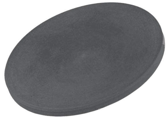
Chromium Nitride Sputtering Target Description
Chromium Nitride (Cr2N) sputtering target, provided by TFM, is a high-quality nitride ceramic material. This material is commonly used in various industrial applications, including coatings for corrosion resistance, wear resistance, and enhanced hardness. It is also employed in the semiconductor industry and for decorative coatings.
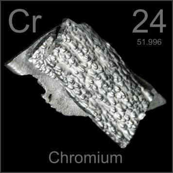 Chromium, represented by the symbol “Cr,” is a chemical element with the atomic number 24. The name originates from the Greek word ‘chroma,’ meaning color, reflecting the many colorful compounds it forms. Chromium has been known and used since ancient times, with historical references dating back to the Terracotta Army era. Positioned in Period 4 and Group 6 of the periodic table, it belongs to the d-block. The relative atomic mass of chromium is 51.9961(6) Dalton, indicating the measurement’s precision.
Related Product: Chromium Sputtering Target
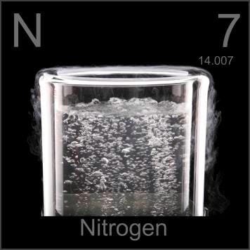 Nitrogen, symbolized as “N,” is a chemical element with the atomic number 7. The name comes from the Greek words ‘nitron’ and ‘genes,’ which mean nitre-forming. It was first identified in 1772 by Daniel Rutherford, who also managed to isolate it. Positioned in Period 2 and Group 15 of the periodic table, nitrogen belongs to the p-block elements. The relative atomic mass of nitrogen is 14.0067(2) Dalton, with the number in brackets representing the uncertainty in this value.
Chromium Nitride Sputtering Target Packaging
Our chromium nitride sputter targets are meticulously handled and packaged to ensure their integrity and quality. We take great care in preventing any potential damage during storage and transportation, thereby preserving the original condition of our products. Each target is clearly tagged and labeled for efficient identification and quality control, ensuring that they arrive in perfect condition for our customers.
Get Contact
TFM offers Chromium Nitride Sputtering Targets in various forms, purities, sizes, and prices. We specialize in high-purity thin film deposition materials with optimal density and minimal grain sizes, which are ideal for semiconductor, CVD, and PVD applications in display and optics. Contact Us for current pricing on sputtering targets and other deposition materials that are not listed.


Reviews
There are no reviews yet.