| Material Type | Chromium Silicate |
| Symbol | CrSiO2 |
| Color/Appearance | Various colors, Solid |
| Melting Point (°C) | N/A |
| Relative Density (g/cc) | >90% |
| Z Ratio | N/A |
| Sputter | RF, DC |
| Max Power Density* (Watts/Square Inch) | |
| Type of Bond | Indium, Elastomer |
| Comments |
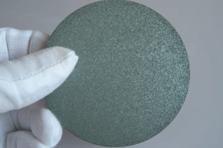
Chromium Silicate Sputtering Targets
Chromium Silicate (CrSiO₄) sputtering targets are high-purity materials used in various advanced applications, particularly in the production of thin films for semiconductor, optics, and electronics industries. These targets are favored for their excellent properties in producing coatings that are resistant to oxidation, wear, and corrosion.
Specifications
- Purity: 99.9%
- Circular Targets: Diameter ≤ 14 inches, Thickness ≥ 1mm
- Block Targets: Length ≤ 32 inches, Width ≤ 12 inches, Thickness ≥ 1mm
Key Features and Advantages
- High Purity: TFM’s Chromium Silicate sputtering targets are made with a purity of 99.9%, ensuring high-quality thin films with consistent and reliable deposition in sensitive applications.
- Custom Sizes Available: These targets are available in custom sizes to meet the specific requirements of both R&D and large-scale production, offering flexibility and adaptability.
- Enhanced Wear Resistance: Chromium Silicate coatings produced from these sputtering targets exhibit enhanced wear and corrosion resistance, making them ideal for use in harsh environments.
- Oxidation Resistance: The material’s ability to resist oxidation makes it suitable for high-temperature applications, contributing to longer-lasting and more reliable performance in various sectors.
- Vacuum Compatible: These targets are thoroughly cleaned and packaged to be compatible with vacuum deposition systems, ensuring protection from environmental contamination during transportation and storage.
Applications
- Semiconductors: Chromium Silicate is used in semiconductor industries to produce thin films that enhance the performance and durability of microelectronic devices.
- Optics: The thin films produced with Chromium Silicate targets are used in optical coatings, offering excellent protection against wear and environmental damage, as well as improved optical properties.
- Electronics: Chromium Silicate thin films are used in electronic components to enhance their durability and reliability, particularly in circuitry and electromagnetic shielding applications.
- Wear-Resistant Coatings: The superior wear resistance of Chromium Silicate makes it an ideal choice for coatings in industrial applications where materials are exposed to abrasion, friction, or extreme conditions.
- Corrosion Protection: The material is also used in coatings that provide corrosion resistance for various metallic surfaces, making it suitable for automotive and aerospace applications.
Manufacturing Process
- Cold-Pressed and Sintered: TFM’s Chromium Silicate sputtering targets are cold-pressed and sintered to achieve high density and uniformity, ensuring efficient and reliable deposition.
- Elastomer Bonding: The sputtering target is elastomer bonded to the backing plate, which improves the durability and handling of the target during the sputtering process.
- Cleaning and Packaging: All targets are cleaned thoroughly and carefully packaged to avoid contamination, ensuring they are ready for vacuum deposition processes in demanding applications.
Available Options
- 99.9% Purity: TFM offers Chromium Silicate sputtering targets with a 99.9% purity to ensure optimal performance in thin film deposition, delivering consistent results across various industries.
- Custom Sizes: Targets are available in a variety of custom sizes to suit specific needs in both small-scale research and large-scale production environments.
- R&D Applications: Smaller sizes of Chromium Silicate sputtering targets are available for research and development (R&D) purposes, offering flexibility for experimentation and prototyping.
- Sputtering Target Bonding Service: TFM provides a bonding service to secure the sputtering target to the backing plate, ensuring enhanced performance in demanding applications.
Conclusion
TFM’s Chromium Silicate Sputtering Targets are ideal for applications requiring wear resistance, oxidation resistance, and high-temperature stability. With their 99.9% purity, customizable sizes, and reliable manufacturing processes, these targets provide high-quality thin films for semiconductor, optics, and electronics industries. Whether used in research, development, or industrial production, Chromium Silicate sputtering targets from TFM deliver consistent, high-performance results across various advanced technologies.


Reviews
There are no reviews yet.