Introduction
Selenium Oxide (SeO₂) Sputtering Targets are specialized ceramic targets used in thin film deposition for semiconductor research, optical materials, and advanced functional coatings. Selenium oxide is a compound known for its unique electronic and optical characteristics, making it valuable in the development of photonic materials, sensors, and experimental semiconductor structures.
In Physical Vapor Deposition (PVD) processes such as RF magnetron sputtering, SeO₂ targets allow the controlled deposition of selenium oxide thin films with stable composition and high purity. These films are often explored in optical coatings, electronic materials research, and specialized thin film devices where selenium-based compounds provide distinctive electrical and photonic behavior.
Detailed Description
Selenium Oxide Sputtering Targets are produced from high-purity selenium oxide powders through advanced ceramic processing techniques such as powder pressing, controlled sintering, and precision machining. These manufacturing methods produce dense and uniform targets that ensure stable sputtering performance and consistent thin film growth.
SeO₂ is a semiconductor-related oxide material with notable optical and chemical characteristics. It exhibits good transparency in certain optical regions and can participate in various chemical interactions, making it useful for experimental thin film systems and photonic applications.
Because SeO₂ is an insulating oxide compound, deposition is typically performed using RF magnetron sputtering, which provides stable plasma conditions and enables the deposition of high-quality oxide films. During sputtering, selenium oxide atoms are ejected from the target surface and deposited onto substrates to form thin films with controlled thickness and composition.
Selenium oxide thin films can exhibit properties such as:
tunable optical characteristics
semiconductor-related electronic behavior
chemical reactivity useful in sensing applications
compatibility with glass and oxide substrates
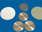
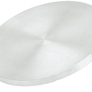
Selenium oxide sputtering targets are available in circular discs, rectangular plates, and custom geometries compatible with most sputtering cathodes. For larger targets or high-power deposition systems, the targets may be bonded to copper backing plates using indium bonding or elastomer bonding to improve thermal stability and mechanical integrity.
High-density targets help maintain stable sputtering rates, reduce particle generation, and ensure uniform thin film deposition.
Applications
Thin films deposited from Selenium Oxide Sputtering Targets are used in several research and technological areas:
Optical coatings – selenium oxide thin films used in specialized optical materials.
Semiconductor research – experimental oxide thin films for electronic devices.
Photonic materials development – optical thin films for photonic systems.
Chemical sensors – thin films used in gas sensing and chemical detection devices.
Thin film electronics – functional layers in experimental electronic devices.
Materials science research – studies involving selenium-based compounds and oxide thin films.
Technical Parameters
| Parameter | Typical Value / Range | Importance |
|---|---|---|
| Purity | 99.9% – 99.99% | Higher purity improves film consistency and optical quality |
| Density | ≥95% theoretical | Ensures stable sputtering performance |
| Diameter | 25 – 300 mm (custom) | Compatible with various sputtering cathodes |
| Thickness | 3 – 6 mm | Influences sputtering rate and target lifetime |
| Bonding | Copper backing plate (optional) | Improves heat transfer and structural stability |
Comparison with Related Materials
| Material | Key Advantage | Typical Application |
|---|---|---|
| Selenium Oxide (SeO₂) | Unique optical and electronic properties | Optical coatings and semiconductor research |
| Selenium (Se) | Semiconductor properties | Photoconductive devices |
| Tellurium Oxide (TeO₂) | Strong optical and acousto-optic characteristics | Optical modulators and photonic devices |
FAQ
| Question | Answer |
|---|---|
| Can SeO₂ sputtering targets be customized? | Yes, diameter, thickness, purity, and backing plate bonding options can be customized according to sputtering system requirements. |
| Which sputtering method is recommended for SeO₂ targets? | RF magnetron sputtering is typically used because selenium oxide is an insulating ceramic material. |
| Are bonded targets available? | Yes, SeO₂ targets can be indium-bonded or elastomer-bonded to copper backing plates for improved thermal management. |
| What substrates are compatible with SeO₂ thin films? | Silicon wafers, glass, quartz, sapphire, and oxide substrates are commonly used. |
| Which industries commonly use SeO₂ sputtering targets? | Semiconductor research laboratories, photonics development centers, sensor technology research, and advanced materials science institutions. |
Packaging
Our Selenium Oxide Sputtering Targets are meticulously tagged and labeled externally to ensure efficient identification and maintain strict quality control standards. Each target is vacuum-sealed and packaged with protective cushioning materials to prevent contamination or mechanical damage during storage and transportation. Export-grade cartons or wooden crates are used to ensure safe international delivery.
Conclusion
Selenium Oxide (SeO₂) Sputtering Targets are advanced ceramic deposition materials used to produce specialized oxide thin films for semiconductor research, optical coatings, and sensor technologies. Their unique electronic and optical characteristics make them valuable for experimental thin film systems and advanced photonic materials.
With high purity, customizable dimensions, and reliable manufacturing processes, SeO₂ sputtering targets provide consistent performance for both research laboratories and industrial thin film deposition systems.
For detailed specifications and a quotation, please contact us at sales@thinfilmmaterials.com.


Reviews
There are no reviews yet.