| Material Type | Tantalum Oxide |
| Symbol | Ta2Ox |
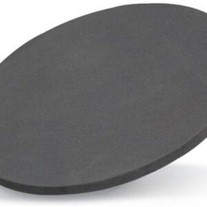
| Color/Appearance | Black, Solid |
| Melting Point (°C) | 1,872 |
| Theoretical Density (g/cc) | 8.2 |
| Z Ratio | 0.3 |
| Sputter | RF, RF-R |
| Max Power Density* (Watts/Square Inch) | 20 |
| Type of Bond | Indium, Elastomer |
| Comments | Slight decomposition. Evaporate Ta in 10-3 Torr O2 |
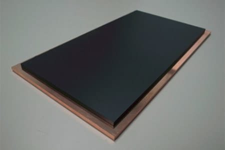
Tantalum Oxide Sputtering Targets
Overview
Tantalum pentoxide (Ta₂O₅), also known as tantalum(V) oxide, is a high-purity, white, inert solid with exceptional properties that make it ideal for advanced applications. It has a high refractive index, low absorption, and is insoluble in solvents, though it is reactive with strong bases and hydrofluoric acid. Ta₂O₅ is commonly used in coatings and the production of capacitors, thanks to its high dielectric constant.
Product Information
- Purity: 99.95%
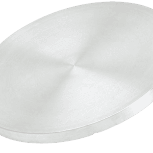
- Circular Dimensions: Diameter ≤ 14 inch, Thickness ≥ 1mm
- Block Dimensions: Length ≤ 32 inch, Width ≤ 12 inch, Thickness ≥ 1mm
Applications
- Ferroelectric
- Gate Dielectric
- For CMOS
Features
- High Purity (99.95% minimum)
- Excellent dielectric properties
- Custom sizes available for various applications
Manufacturing Process
- Cold pressed and sintered
- Elastomer bonded to backing plate
- Cleaned for vacuum use, with protection against environmental contaminants during shipment
Options
- 99.95% minimum purity
- Smaller sizes available for R&D applications
- Sputtering target bonding service available
TFM offers high-quality Tantalum Oxide Sputtering Targets suitable for a wide range of applications, including thin film deposition and capacitor production.

Reviews
There are no reviews yet.