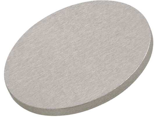
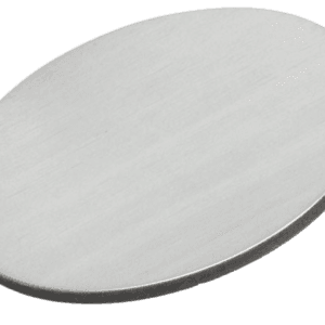
Titanium Silicide Sputtering Target Description
Titanium silicide sputtering target is a silicide ceramic sputtering material composed of titanium and silicon. This material is commonly used in various applications, particularly in thin film deposition processes. The combination of titanium and silicon in the target allows for the creation of films with desirable properties for use in the semiconductor, display, and photovoltaic industries, among others.
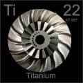 Titanium is a chemical element named after the Titans of Greek mythology, symbolizing strength. It was first discovered in 1791 by William Gregor, with its isolation and identification as a unique element later confirmed by Jöns Jakob Berzelius. The chemical symbol for titanium is “Ti,” and it is located in Period 4, Group 4 of the periodic table, classified within the d-block. Titanium has an atomic number of 22 and a relative atomic mass of 47.867(1) Dalton, with the number in brackets indicating the uncertainty in its measurement.
Related Product: Titanium Sputtering Target
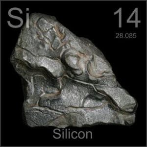 Silicon is a chemical element named after the Latin word ‘silex’ or ‘silicis,’ meaning flint. It was first described in 1824 by Jöns Jakob Berzelius, who also achieved its isolation. The chemical symbol for silicon is “Si,” and it is found in Period 3 and Group 14 of the periodic table, part of the p-block. Silicon has an atomic number of 14, and its relative atomic mass is 28.0855(3) Dalton, with the number in brackets indicating the measurement’s uncertainty.
Titanium Silicide Sputtering Target Application
The titanium silicide sputtering target is utilized in various applications, including thin film deposition, decorative coatings, and the production of semiconductor components. It is commonly used in displays, LED devices, photovoltaic cells, and functional coatings. Additionally, it finds applications in the optical information storage industry, glass coatings for automotive and architectural uses, and optical communication systems.
Titanium Silicide Sputtering Target Packing
Our titanium silicide sputter targets are meticulously tagged and labeled externally to ensure easy identification and maintain stringent quality control. We take special precautions to protect these targets from damage during storage and transportation, ensuring they arrive in perfect condition.

Reviews
There are no reviews yet.