
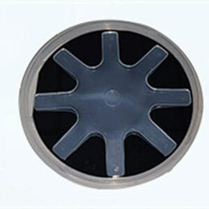
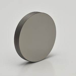
TFM Silicon Carbide Wafer: Advanced Materials for a High-Tech Future
TFM leads the way in Silicon Carbide (SiC) wafer production, providing unparalleled quality and innovation for high-tech industries. Our expertise, combined with state-of-the-art technology, allows us to deliver SiC wafers tailored to meet the dynamic demands of modern applications.
At TFM, we pride ourselves on customization and precision, ensuring that our wafers provide the ideal solution for your specific needs, helping to drive the future of advanced technology.
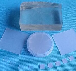
Silicon Carbide Wafer Specifications
| Specification | Details |
|---|---|
| Size | 10×3 mm, 10×5 mm, 10×10 mm, 15×15 mm, 20×15 mm, 20×20 mm, Dia 15 mm, Dia 20 mm, Dia 1″, Dia 2″, Dia 4″, Dia 6″ |
| Thickness | 0.35 mm |
| Crystal Orientation | <0001> |
| Polished | SSP or DSP |
| Redirection Precision | ±0.5° |
| Edge Redirection | 2° (special in 1°) |
| Angle of Crystalline | Special sizes and orientations available upon request |
| Surface Roughness (Ra) | ≤ 5 Å (5 μm × 5 μm) |
Silicon Carbide Wafer Physical Properties
| Property | Details |
|---|---|
| Material | SiC |
| Growth Method | MOCVD |
| Crystal Structure | M6 |
| Lattice (Å) | a = 3.08, c = 15.08 |
| Direction | <0001> 3.5º |
| Density (g/cm³) | 3.21 g/cm³ |
| Hardness (Mohs) | 9.2 |
| Melting Point | 1900°C |
| Heat Traveling @300K | 5 W/cm·K |
| Dielectric Constants | e(11) = e(22) = 9.66, e(33) = 10.33 |
Choose TFM’s Silicon Carbide wafers for your next-generation applications, offering exceptional performance, reliability, and precision to meet the future of advanced semiconductor technology.
Reviews
There are no reviews yet.