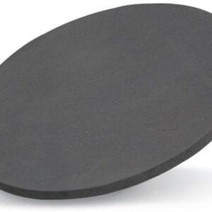
Indium Sulfide Sputtering Target Description


The indium sulfide sputtering target is a type of ceramic sputtering material made from indium and sulfur. This material is commonly used in various industrial applications, particularly for creating thin films. It offers a unique combination of properties that make it suitable for use in advanced electronic and optoelectronic devices, including displays, LEDs, and photovoltaic cells. Indium sulfide is valued for its ability to form high-quality films with good electrical and optical characteristics.
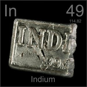 Indium is a chemical element that derives its name from the Latin word ‘indicium,’ meaning violet or indigo, reflecting the color of its spectral lines. It was first identified in 1863 by F. Reich and T. Richter, who also successfully isolated the element. Indium is represented by the chemical symbol “In” and has an atomic number of 49. It is positioned in Group 13 and Period 5 of the periodic table, belonging to the p-block elements. The relative atomic mass of indium is 114.818(3) Dalton, with the number in brackets indicating the uncertainty in the measurement.
Related Product: Indium Sputtering Target
 Sulfur, also known as sulphur, is a chemical element with a rich history, dating back to before 2000 BC, where it was used and discovered by ancient Chinese and Indian civilizations. The name sulfur derives from either the Sanskrit word ‘sulvere’ or the Latin ‘sulfurium,’ both referring to sulfur. Its chemical symbol is “S,” and it is positioned in Group 16 and Period 3 of the periodic table, part of the p-block. Sulfur has an atomic number of 16 and a relative atomic mass of 32.065(5) Dalton, with the value in brackets indicating the uncertainty of the measurement.
Indium Sulfide Sputtering Target Specification
| Compound Formula | In2S3 |
| Appearance | Solid |
| Melting Point | 1,050° C |
| Density | 4.90 g/cm3 |
| Available Sizes | Dia.: 1.0″, 2.0″, 3.0″, 4.0″, 5.0″, 6.0″ Thick: 0.125″, 0.250″ |
Indium Sulfide Sputtering Target Application
The indium sulfide sputtering target is widely utilized in various applications, including thin film deposition and decorative coatings. It’s especially valuable in the semiconductor, display, LED, and photovoltaic industries, where it serves as a functional coating material. Additionally, it finds use in optical information storage, glass coating for automotive and architectural purposes, and optical communication systems. These applications leverage the unique properties of indium sulfide to enhance the performance and durability of coated surfaces.
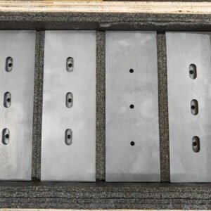
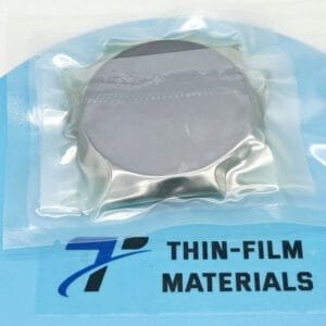
Indium Sulfide Sputtering Target Packing
Our indium sulfide sputter targets are meticulously tagged and labeled externally to ensure efficient identification and stringent quality control. We take great care in packaging to prevent any potential damage during storage or transportation, thereby preserving the integrity and quality of the product.
Get Contact
TFM offers Indium Sulfide Sputtering Targets in various forms, purities, sizes, and prices. We specialize in high-purity thin film deposition materials with optimal density and minimal grain sizes, which are ideal for semiconductor, CVD, and PVD applications in display and optics. Contact Us for current pricing on sputtering targets and other deposition materials that are not listed.
Reviews
There are no reviews yet.