
Copper Sulfide Sputtering Target Description
Copper sulfide sputtering targets are ceramic materials composed of copper (Cu) and sulfur (S). These targets are used in various thin film deposition processes, including semiconductor manufacturing, display technology, and photovoltaic devices. Copper sulfide thin films are valued for their electrical properties and are often used in applications requiring p-type semiconductors or as part of multi-layer structures for solar cells and other electronic devices.
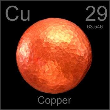 Copper is a chemical element with the symbol “Cu,” derived from the Old English word “coper,” which itself comes from the Latin term “Cyprium aes,” meaning “metal from Cyprus.” Copper has been used by humans since approximately 9000 BC, with early uses traced back to the Middle East. It is found in the periodic table at atomic number 29, situated in Period 4 and Group 11, belonging to the d-block of transition metals. Copper has a relative atomic mass of 63.546(3) Dalton, with the number in brackets indicating the uncertainty in this value.
Related Product: Copper Sputtering Target
 Sulfur, also known as sulphur, is a chemical element that has been known and used since ancient times, with its name possibly derived from the Sanskrit word “sulvere” or the Latin “sulfurium.” It was widely recognized before 2000 BC and was notably used by ancient Chinese and Indian civilizations. The chemical symbol for sulfur is “S,” and it is found in the periodic table at atomic number 16, located in Period 3 and Group 16, part of the p-block elements. The relative atomic mass of sulfur is 32.065(5) Dalton, with the number in brackets indicating the uncertainty in this measurement.
Copper Sulfide Sputtering Target Specification
| Material Type | Copper Sulfide |
| Symbol | CuS |
| Color/Appearance | Black target |
| Melting Point | 500 °C (932 °F) |
| Density | 4.6 g/cm3 |
| Sputter | RF, RF-R |
| Type of Bond | Indium, Elastomer |
Copper Sulfide Sputtering Target Target Bonding
Specialized bonding services for Copper Sulfide Sputtering Targets, including indium and elastomeric bonding techniques, enhance performance and durability. Thin Film Materials (TFM) ensures high-quality solutions that meet industry standards and customer needs.
We also offer custom machining of backing plates, which is essential for sputtering target assembly. This comprehensive approach improves target design flexibility and performance in thin film deposition. Our channels provide detailed information about bonding materials, methods, and services, helping clients make informed decisions.

Packing
Our copper sulfide sputtering targets are carefully tagged and labeled externally to ensure efficient identification and quality control. We take great care in handling and packaging to prevent any damage during storage or transportation, ensuring that the product arrives in optimal condition.
Get Contact
TFM offers Copper Sulfide Sputtering Targets in various forms, purities, sizes, and prices. We specialize in high-purity thin film deposition materials with optimal density and minimal grain sizes, which are ideal for semiconductor, CVD, and PVD applications in display and optics. Contact Us for current pricing on sputtering targets and other deposition materials that are not listed.


Reviews
There are no reviews yet.