
 MSDS File
| Material Type | GeSbTe |
| Symbol | GeSbTe |
| Melting Point (°C) | |
| Theoretical Density (g/cc) |
| Z Ratio | |
| E-Beam | |
| E-Beam Crucible Liner Material | |
| Temp. (°C) for Given Vap. Press. (Torr) | |
| Comments |
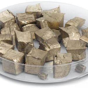
GeSbTe Pellet Evaporation Material
TFM offers high-purity GeSbTe Pellet Evaporation Material, a key material for thin-film deposition in phase-change memory (PCM) devices, optical recording, and semiconductor applications. Composed of germanium (Ge), antimony (Sb), and tellurium (Te), this material features unique phase-change properties that enable reversible transitions between amorphous and crystalline states, making it ideal for use in data storage technologies and optical devices.
Designed for thermal evaporation and electron beam (E-beam) evaporation, GeSbTe Pellet Evaporation Material ensures uniform deposition, high film purity, and excellent adhesion. This material is well-suited for the development of high-performance memory devices, photonic systems, and optical storage media.
Key Features and Advantages
Reversible Phase-Change Properties: Ideal for phase-change memory (PCM) and optical recording applications where the material can switch between amorphous and crystalline states for reliable data storage and retrieval.
High Purity & Excellent Film Uniformity: Ensures consistent deposition, reducing defects and improving device reliability.
Fast Switching Speed: Facilitates fast data storage and retrieval in optical and memory devices, providing enhanced performance for non-volatile memory systems.
Superior Adhesion & Smooth Coatings: Guarantees strong film adhesion and smooth surface coatings for high-quality device performance.
Custom Compositions Available: Tailored to meet specific needs for research, development, and industrial applications.
Applications
Phase-Change Memory (PCM): Used in next-generation non-volatile memory devices, offering fast read/write speeds and high-density storage.
Optical Data Storage: Ideal for optical recording applications such as CDs, DVDs, Blu-ray, and rewritable optical disks.
Semiconductor & Photonic Devices: Plays a critical role in photonic systems, laser technologies, and advanced semiconductor research.
Thin-Film Coatings for Optical Systems: Essential for optical coatings used in data storage systems and high-tech optical devices.
Industry Impact and Customization
TFM’s GeSbTe Pellet Evaporation Material supports the development of high-performance data storage and optical recording systems. With precise composition control, high purity, and uniform deposition, TFM provides material solutions that enable the advancement of phase-change memory technology and next-generation optical storage.
With its unique phase-change properties, superior film quality, and exceptional performance, TFM’s GeSbTe Pellet Evaporation Material is a crucial component for innovative memory devices, optical data storage technologies, and advanced semiconductor applications, ensuring outstanding efficiency, long-term reliability, and consistent high performance.


Reviews
There are no reviews yet.