
 MSDS File
Introduction
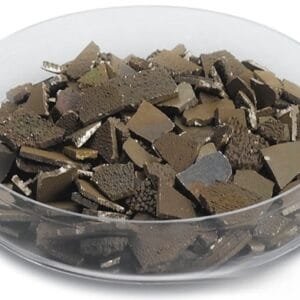
Mercury Sulfide Pellet Evaporation Material is a specialized compound used in thin film research and niche optical or electronic applications where controlled sulfur–mercury chemistry is required. Supplied in pellet form, HgS (commonly known as cinnabar in its stable phase) supports reproducible evaporation behavior and precise material delivery in Physical Vapor Deposition (PVD) processes under carefully controlled conditions.
Detailed Description
Mercury sulfide evaporation materials are produced with strict control over stoichiometry, phase stability, and impurity levels. Pelletized geometry is selected to ensure uniform heating, reduced spitting, and predictable evaporation rates when used in thermal evaporation sources or compatible crucibles.
Due to the volatility of mercury-containing compounds, material preparation and handling are carried out under controlled environments to minimize contamination and ensure operator safety. Pellet size and density are optimized to match common evaporation boats and crucibles, helping maintain stable flux during deposition. Customized pellet dimensions and purity grades are available to align with specific research protocols and equipment configurations.
Each batch is processed to support consistent film composition, which is critical for optical absorption characteristics, electronic behavior, and experimental repeatability in HgS-based thin films.
Applications
Optical and optoelectronic material research
Sulfide-based compound thin film studies
Experimental semiconductor and sensor coatings
Specialized academic and laboratory PVD research
Reference material deposition and materials science investigations
Technical Parameters
| Parameter | Typical Value / Range | Importance |
|---|---|---|
| Material | Mercury Sulfide (HgS) | Functional sulfide compound |
| Purity | 99.9% – 99.99% | Controls film consistency |
| Form | Pellets | Stable evaporation and handling |
| Pellet Size | Customizable (typ. 1–6 mm) | Matches evaporation sources |
| Evaporation Method | Thermal evaporation | Compatible with PVD systems |
| Packaging | Vacuum-sealed / inert atmosphere | Prevents contamination |
Comparison with Related Materials
| Material | Key Advantage | Typical Application |
|---|---|---|
| Mercury Sulfide (HgS) | Stable Hg–S compound | Optical & research films |
| Zinc Sulfide (ZnS) | Non-toxic, optical clarity | Optical coatings |
| Cadmium Sulfide (CdS) | Semiconductor properties | Photodetectors & optoelectronics |
FAQ
| Question | Answer |
|---|---|
| Can pellet size and purity be customized? | Yes, pellet dimensions and purity grades can be tailored. |
| Is HgS suitable for thermal evaporation? | Yes, under controlled conditions and appropriate source design. |
| How is safety handled during shipping? | Materials are sealed, labeled, and packed in compliance with regulations. |
| Which users typically require HgS pellets? | Academic labs, research institutes, and specialized R&D facilities. |
| Is documentation provided? | Certificate of Analysis is available upon request. |
Packaging
Our Mercury Sulfide Pellet Evaporation Materials are meticulously labeled and vacuum-sealed or packed under inert atmosphere to maintain material integrity. Protective cushioning and export-compliant packaging are used to ensure safe transportation and storage.
Conclusion
Mercury Sulfide Pellet Evaporation Material offers controlled composition, stable evaporation behavior, and flexible customization for specialized thin film research. With careful processing, secure packaging, and documentation support, it is well suited for advanced laboratory and experimental PVD applications.
For detailed specifications and a quotation, please contact us at sales@thinfilmmaterials.com.


Reviews
There are no reviews yet.