
")


Introduction
Thin film technology is the backbone of modern electronics, semiconductor devices, and optoelectronics. The thin film substrate plays a crucial role in determining the performance and stability of thin films used in applications like semiconductors, high-power electronics, sensors, and nanotechnology.
Whether you’re working with semiconductor wafers, ceramic substrates, or metal thin films, choosing the right substrate is critical for achieving high-quality, reliable results. In this article, we will explore the types of thin film substrates, their materials and properties, and their applications in advanced industries.
Table of Contents
What Is a Thin Film Substrate?
A thin film substrate is the foundational material on which a thin layer of another substance is deposited. The substrate supports the thin film and ensures stability, adhesion, and electrical performance.
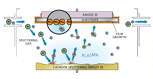
Thin film substrates are used in various deposition techniques, including:
- Physical Vapor Deposition (PVD) – Used for high-purity coatings in microelectronics.
- Chemical Vapor Deposition (CVD) – Used in semiconductor manufacturing and optics.
- Sputtering – A method to create uniform coatings for sensors, displays, and wear-resistant surfaces.
What Are the Substrates for ATP Thin Film?
ATP (Advanced Thin Film Processing) requires high-performance substrates that can withstand precise and demanding deposition processes. ATP thin film applications are commonly found in high-tech industries such as semiconductors, optoelectronics, and advanced coatings.
Common Substrates for ATP Thin Films
- Silicon (Si) Wafers – Used in microelectronics, sensors, and photonics for their electrical properties and compatibility with integrated circuits.
- Gallium Nitride (GaN) & Silicon Carbide (SiC) Substrates – Essential for high-frequency and power electronics, particularly in 5G, RF devices, and laser diodes. GaN-on-Si substrates are widely used in power electronics and LEDs, combining the advantages of silicon processing with GaN’s high electron mobility.
- Sapphire & Ceramic Substrates – Found in LED manufacturing and high-temperature applications, providing excellent thermal and optical properties.
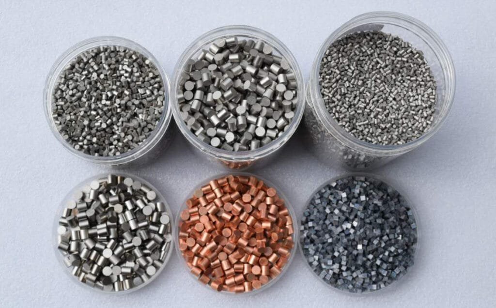
- Metal Substrates (Tungsten, Molybdenum, Titanium, Tantalum) – Used for thin film resistors, high-temperature coatings, and aerospace applications.
- Superconducting Materials (Niobium, Hafnium, Vanadium) – Used in quantum computing, superconducting circuits, and cryogenic electronics.
- Halide Crystal Substrates (CaF₂, MgF₂) – Found in IR optics and spectroscopy, used for their ultra-high transparency in UV and infrared ranges.
What Are Thin Film Modules?
A thin film module is a functional unit that integrates thin film technology into a device or component. Thin film modules are widely used in electronics, energy systems, and optoelectronics.
Types of Thin Film Modules & Applications
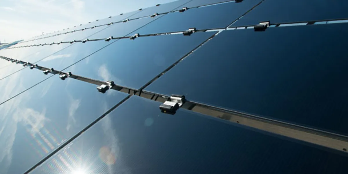
Thin Film Solar Modules
- Application: CIGS (Copper Indium Gallium Selenide) and CdTe (Cadmium Telluride) solar cells use thin film layers on glass or metal substrates.
- Why It Matters: Lightweight, flexible, and cost-effective compared to traditional silicon solar panels.
- Example: First Solar and Hanergy produce thin-film photovoltaic panels for commercial energy solutions.
Thin Film Transistor (TFT) Modules
- Application: Used in LCDs, OLED displays, and flexible electronics.
- Why It Matters: Provides high-speed switching, low power consumption, and excellent image quality.
- Example: Samsung and LG use TFT thin film modules in OLED and LCD displays.
Thin Film Sensors & MEMS Modules
- Application: Used in biosensors, pressure sensors, and gas detection.
- Why It Matters: Enables ultra-sensitive detection in healthcare, industrial monitoring, and environmental applications.
- Example: Bosch and Texas Instruments develop MEMS-based thin film sensors for IoT and automotive applications.
Thin Film Supercapacitor & Battery Modules
- Application: Found in wearable electronics, EV batteries, and energy storage.
- Why It Matters: Provides high energy density, long life cycles, and flexibility for compact devices.
- Example: Panasonic and Tesla are investing in thin film battery technology for next-gen EVs.
Types of Thin Film Substrates
Thin film substrates can be categorized into seven major types based on their material composition and application areas:
1. Semiconductor Substrates
These are the most widely used substrates in integrated circuits (ICs), transistors, and memory devices. Silicon wafers (Si), gallium arsenide (GaAs), and silicon carbide (SiC) are the most common semiconductor substrates due to their high electrical performance and thermal stability.
2. GaN Thin Film Substrates
Gallium nitride (GaN) substrates are crucial for high-power electronics, RF devices, and optoelectronic applications. GaN thin film substrates provide high electron mobility, excellent thermal conductivity, and superior efficiency in high-frequency applications such as 5G technology and laser diodes.
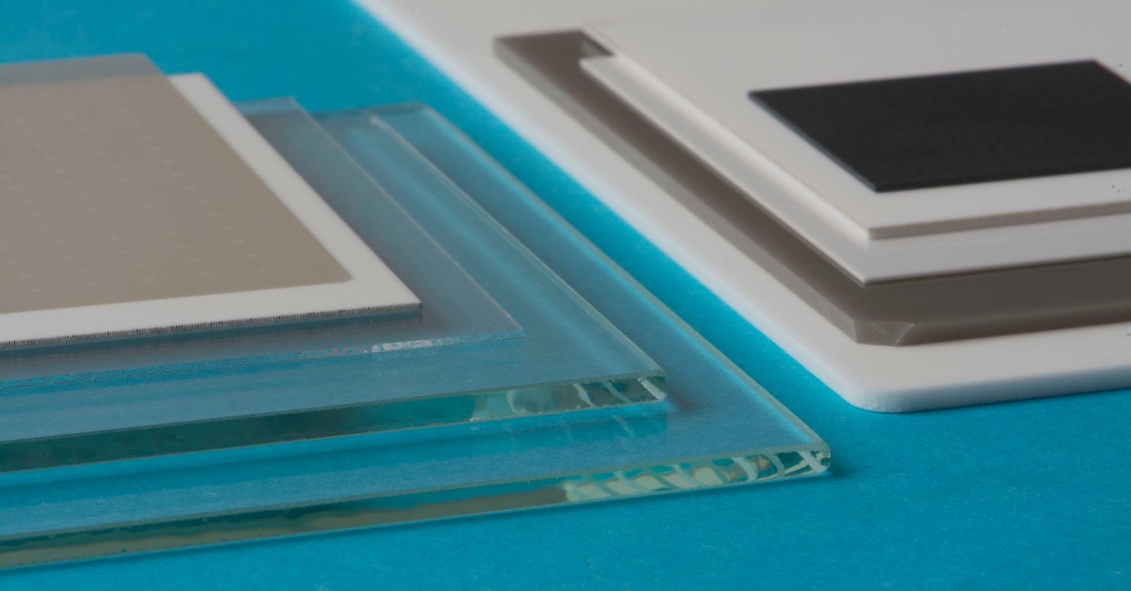
3. Ceramic Substrates
Ceramic-based thin film substrates, including aluminum oxide (Al₂O₃), zirconium oxide (ZrO₂), and hafnium oxide (HfO₂), are used in insulating layers for microelectronics, high-dielectric capacitors, and high-temperature applications. These substrates are widely used in LED manufacturing, power electronics, and aerospace components.
4. Halide Crystal Substrates
Halide crystal substrates, such as potassium bromide (KBr) and calcium fluoride (CaF₂), are used in infrared (IR) optics, spectroscopy, and laser applications. Their high optical transparency in the UV, visible, and IR spectrums makes them essential in optical sensors and imaging systems.
5. High-Temperature Superconducting Thin Film Substrates
These substrates, such as yttrium barium copper oxide (YBCO) and niobium-based compounds, are used for quantum computing, superconducting circuits, and next-generation energy storage solutions. They provide zero electrical resistance at extremely low temperatures, making them valuable for MRI machines and cryogenic electronics.
6. Magnetic and Ferroelectric Thin Film Substrates
Used in data storage devices, spintronic applications, and memory chips, these substrates include materials such as barium titanate (BaTiO₃), lead zirconate titanate (PZT), and ferrites. They allow precise polarization control and play a significant role in magnetic sensors and advanced memory devices.
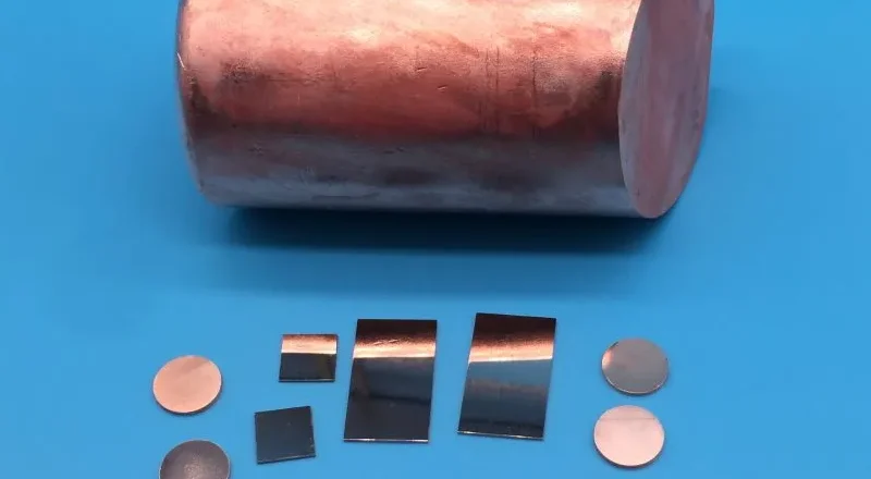
7. Metal Substrates
Metal thin film substrates include tungsten (W), molybdenum (Mo), tantalum (Ta), and titanium (Ti). They are widely used in wear-resistant coatings, high-temperature applications, and electronic shielding. Metal substrates provide excellent conductivity and durability for aerospace, defense, and advanced industrial applications.
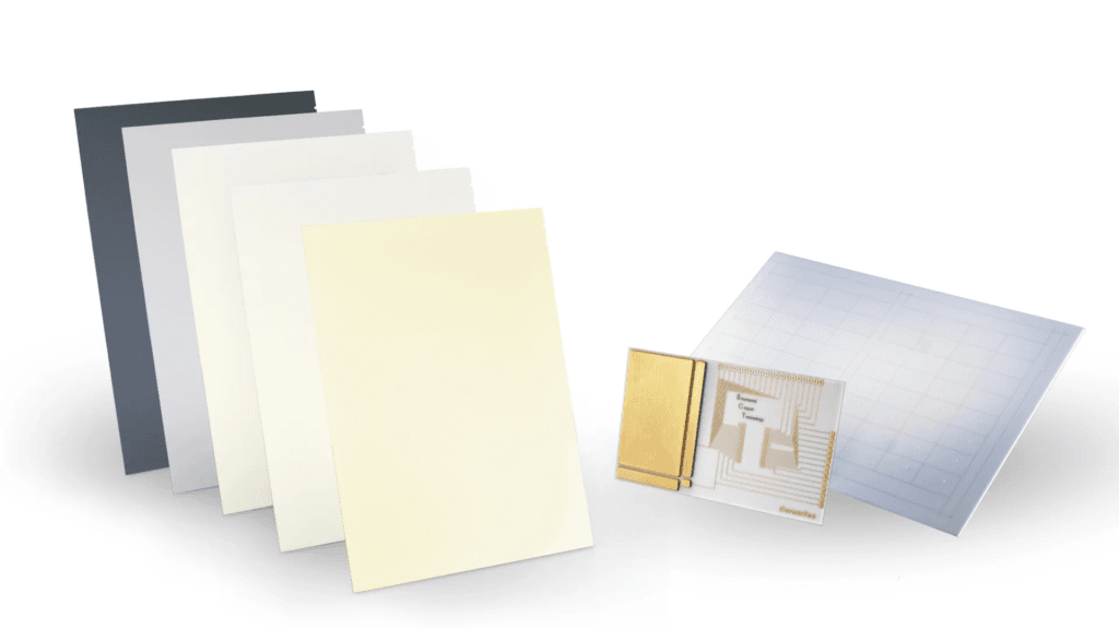
Materials Used in Thin Film Substrates
The selection of a substrate depends on its mechanical, thermal, and electrical properties. Here are the most common materials used:
1. Semiconductor Materials
- Silicon (Si): The most common material for microelectronics and integrated circuits.
- Gallium Nitride (GaN): Used for high-frequency electronics and laser diodes.
- Silicon Carbide (SiC): Preferred for power electronics and high-temperature applications.
2. Refractory Metals
- Tungsten (W): High melting point, used in microelectronics and wear-resistant coatings.
- Molybdenum (Mo): Used in solar panels and semiconductor devices.
- Tantalum (Ta): Corrosion-resistant, ideal for capacitors and biomedical coatings.
3. Oxide and Ceramic Materials
- Hafnium Oxide (HfO₂): Used in high-dielectric applications and gate oxides in transistors.
- Zirconium Oxide (ZrO₂): Applied in optical coatings and high-temperature electronics.
4. Magnetic and Superconducting Materials
- Niobium (Nb) and Niobium Nitride (NbN): Used in quantum computing and superconducting circuits.
- Barium Titanate (BaTiO₃): A ferroelectric material used in data storage and piezoelectric devices.
5. Metal Thin Film Substrates
- Titanium (Ti): Provides high strength and corrosion resistance for medical devices and aerospace applications.
- Vanadium (V): Used in optical coatings and thin-film transistors.
Key Properties of Thin Film Substrates
The ideal thin film substrate must meet specific physical, chemical, and electrical criteria, including:
- Thermal Stability – Can withstand high temperatures without deformation.
- Chemical Resistance – Should resist oxidation and chemical degradation.
- Mechanical Strength – Supports thin films without cracking.
- Surface Smoothness – Ensures uniform thin film deposition.
- Electrical Conductivity or Insulation – Depending on the application, it should be conductive (e.g., metal substrates) or insulating (e.g., ceramic substrates).
Why Are Thin Film Substrates Important?
Thin film substrates play a crucial role in:
- Microelectronics & Semiconductors – Used in transistors, memory chips, and integrated circuits.
- Optoelectronics – Essential for LEDs, laser diodes, and optical coatings.
- Nanotechnology & Quantum Computing – Provide a platform for superconducting materials and nanoscale components.
- Aerospace & High-Temperature Applications – Used for wear-resistant coatings and thermal protection.
- Energy & Solar Cells – Form the foundation for photovoltaic thin-film solar technology.
Applications of Thin Film Substrates
Thin film substrates are widely used in various industries, playing a critical role in the development of semiconductors, microelectronics, optoelectronics, energy solutions, and high-tech coatings. Below are some real-world examples of how thin film substrates are applied:
1. Semiconductors & Microelectronics
Example: Silicon Wafers in Integrated Circuits (ICs)
- Application: Silicon (Si) wafers serve as the primary substrate for fabricating transistors, processors, and memory chips used in computers, smartphones, and other electronic devices.
- Why It Matters: Silicon provides excellent electrical conductivity, thermal stability, and precise microfabrication compatibility.
- Real-World Use: Intel, TSMC, and Samsung use high-purity silicon wafers as substrates for their advanced semiconductor manufacturing.
2. Optoelectronics
Example: GaN Thin Film Substrates for LED Technology
- Application: Gallium Nitride (GaN) thin film substrates are used in LED (Light Emitting Diode) displays and laser diodes.
- Why It Matters: GaN provides high electron mobility, superior thermal management, and excellent efficiency, making it ideal for energy-efficient lighting and high-brightness displays.
- Real-World Use: Sony and LG use GaN-based thin film substrates in their LED TVs and laser projectors.
3. Energy & Solar Cells
Example: Molybdenum Substrates in Thin Film Solar Panels
- Application: Molybdenum (Mo) thin film substrates act as a conductive back layer in CIGS (Copper Indium Gallium Selenide) solar cells.
- Why It Matters: Mo is highly conductive, corrosion-resistant, and compatible with solar absorption layers, increasing panel efficiency.
- Real-World Use: First Solar and Hanergy use molybdenum substrates for high-efficiency thin-film solar panels.
4. Aerospace & High-Temperature Applications
Example: Tungsten Thin Films for Rocket Engine Coatings
- Application: Tungsten (W) thin films are deposited onto aerospace components to improve thermal resistance and durability.
- Why It Matters: Tungsten’s high melting point (3422°C) and extreme wear resistance make it ideal for rocket engine nozzles and high-speed turbine blades.
- Real-World Use: NASA and SpaceX utilize tungsten coatings in spacecraft thermal protection systems.
5. Nanotechnology & Quantum Computing
Example: Niobium-Based Superconducting Thin Films for Quantum Processors
- Application: Niobium Nitride (NbN) substrates are used to fabricate superconducting qubits in quantum computers.
- Why It Matters: NbN thin films exhibit zero electrical resistance at cryogenic temperatures, enabling high-speed quantum calculations with minimal energy loss.
- Real-World Use: IBM and Google Quantum AI use niobium-based thin film substrates in their superconducting quantum computers.
6. Medical & Biosensors
Example: Titanium Thin Films in Medical Implants
- Application: Titanium (Ti) thin film coatings are used in biomedical implants, such as hip replacements and pacemaker components.
- Why It Matters: Titanium is biocompatible, corrosion-resistant, and integrates well with human tissue, reducing implant rejection.
- Real-World Use: Medtronic and Johnson & Johnson use titanium-coated implants in orthopedic and cardiovascular medical devices.
7. Optical Coatings & Display Technology
Example: Zirconium Oxide (ZrO₂) for Anti-Reflective Lenses
- Application: Zirconium Oxide (ZrO₂) thin films are used in anti-reflective coatings for glasses, camera lenses, and optical sensors.
- Why It Matters: ZrO₂ enhances light transmission, reduces glare, and improves optical clarity.
- Real-World Use: Canon and Nikon use ZrO₂-based coatings in high-performance camera lenses.
Sum Up
Choosing the right thin film substrate is essential for optimizing performance in electronics, semiconductors, and nanotechnology. Whether it’s silicon wafers, refractory metal substrates, or ceramic substrates, each material has distinct advantages tailored to specific applications.
If you’re looking for high-purity thin film substrate materials, custom wafer solutions, or specialized evaporation products, TFM provides industry-leading solutions. Contact Us today to find the perfect substrate for your application!