Introduction
Lanthanum Aluminate (LaAlO₃) substrate is a perovskite-structured single crystal widely used in advanced oxide electronics, superconducting films, microwave devices, and epitaxial thin-film research. Owing to its excellent lattice compatibility with many functional oxide materials, LaAlO₃ has become a key platform for heterostructure engineering, particularly in high-temperature superconductors and ferroelectric or multiferroic systems.
Its combination of thermal stability, chemical durability, and dielectric performance makes LaAlO₃ substrates highly suitable for both academic research and industrial thin-film production.
Detailed Description
Lanthanum Aluminate crystallizes in a distorted perovskite structure and is typically supplied as single-crystal wafers with precise crystallographic orientations such as (100), (110), or (111). The lattice parameter (~3.79 Å pseudo-cubic) enables close lattice matching with materials like YBa₂Cu₃O₇₋δ (YBCO), SrTiO₃-based films, and various rare-earth oxides, minimizing strain and defect density during epitaxial growth.
High-quality LaAlO₃ substrates are grown using controlled crystal growth techniques such as the Czochralski method to ensure:
Low dislocation density
Uniform lattice constant
Minimal twinning
Excellent surface flatness
Typical substrates are available in single-side polished (SSP) or double-side polished (DSP) formats, with surface roughness (Ra) at the nanometer level to support high-quality thin-film deposition. The dielectric constant and low microwave loss characteristics further enhance its suitability in RF and microwave applications.
Compared with some alternative oxide substrates, LaAlO₃ offers higher dielectric permittivity and better lattice compatibility for many perovskite films, enabling improved film crystallinity and functional performance.
Applications
Lanthanum Aluminate substrates are widely applied in:
High-Temperature Superconducting Films
Ideal for YBCO and other REBCO superconducting thin films used in power transmission and sensing devices.Oxide Electronics & 2D Electron Gas (2DEG) Research
LaAlO₃/SrTiO₃ heterostructures are extensively studied for interface conductivity and emergent quantum phenomena.Ferroelectric and Multiferroic Thin Films
Supports epitaxial growth of complex oxides used in memory devices and sensors.Microwave and RF Components
Beneficial dielectric properties make it suitable for resonators, filters, and dielectric substrates.Optical and Laser Devices
Used as a host material and substrate for epitaxial optical films.Research & Development Platforms
Commonly used in universities and national laboratories for thin-film deposition studies including PLD, MBE, and sputtering.
Technical Parameters
| Parameter | Typical Value / Range | Importance |
|---|---|---|
| Crystal Structure | Perovskite (Rhombohedral) | Enables lattice matching with oxide films |
| Orientation | (100), (110), (111) | Determines epitaxial growth behavior |
| Lattice Constant | ~3.79 Å (pseudo-cubic) | Controls film strain and interface quality |
| Surface Roughness (Ra) | < 0.5 nm (polished surface) | Critical for high-quality thin films |
| Thickness | 0.2 – 1.0 mm (custom) | Mechanical stability & handling |
| Diameter / Size | 5×5 mm – 2″ (custom) | Matches deposition systems |
| Polishing | SSP / DSP | Required for specific film processes |
Comparison with Related Materials
| Material | Key Advantage | Typical Application |
|---|---|---|
| Lanthanum Aluminate | Excellent lattice match for YBCO | Superconducting films |
| Strontium Titanate | Tunable dielectric properties | Oxide electronics |
| Sapphire (Al₂O₃) | High thermal conductivity & hardness | LED and optical films |
| Magnesium Oxide | Good high-temperature stability | Magnetic and oxide films |
LaAlO₃ is often selected when precise lattice matching and dielectric performance are prioritized over mechanical hardness.
FAQ
| Question | Answer |
|---|---|
| Can the substrate orientation be customized? | Yes, (100), (110), (111), and other orientations can be supplied upon request. |
| Is double-side polishing available? | Yes, both SSP and DSP options are offered depending on deposition requirements. |
| What deposition methods are compatible? | Suitable for PLD, MBE, RF/DC sputtering, and CVD processes. |
| Can you provide small R&D sizes? | Yes, small square substrates and custom dimensions are available. |
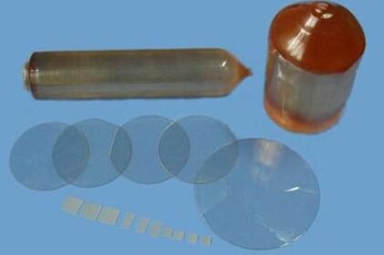
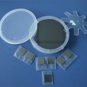
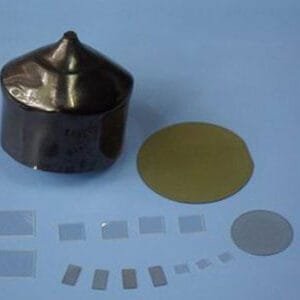
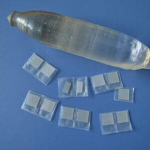
| How are the substrates packaged? | Individually vacuum-packed with cleanroom-grade protection to avoid contamination and chipping. |
Packaging
Our Lanthanum Aluminate Substrates are meticulously tagged and labeled externally to ensure efficient identification and maintain high standards of quality control. We take great care to prevent any potential damage during storage and transportation, ensuring the substrates arrive in perfect condition.
Conclusion
Lanthanum Aluminate (LaAlO₃) substrate remains a cornerstone material for epitaxial oxide thin films and superconducting technologies. With controlled crystal growth, precise orientation, and high-quality polishing, it provides a stable and reliable platform for advanced functional materials research and industrial device fabrication.
For detailed specifications and a quotation, please contact us at sales@thinfilmmaterials.com.
Reviews
There are no reviews yet.