Introduction
Terbium Gallium Garnet (TGG, Tb₃Ga₅O₁₂) substrates are widely recognized as one of the most important magneto-optical materials used in modern photonics and laser systems. With an exceptionally high Verdet constant and excellent optical transparency in the visible and near-infrared range, TGG substrates play a critical role in optical isolators, Faraday rotators, and advanced laser protection systems. They are especially valued in high-power and high-stability optical environments where precise control of polarization is required.
Detailed Description
TGG is a cubic garnet crystal with outstanding magneto-optical performance, combining strong Faraday rotation with good thermal conductivity and mechanical stability. Compared with many other magneto-optical crystals, TGG offers a superior balance between optical clarity, thermal resistance, and long-term reliability under intense laser irradiation.
High-quality TGG substrates are grown using carefully controlled crystal growth techniques to ensure uniform composition, low birefringence, and minimal internal stress. The cubic crystal structure allows for isotropic optical behavior, which simplifies optical system design and improves repeatability in precision devices.
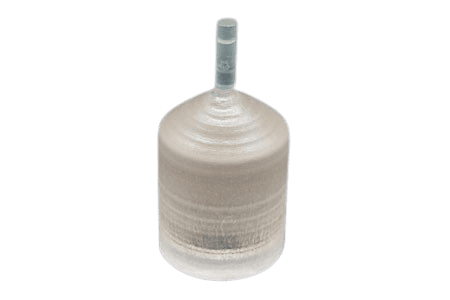
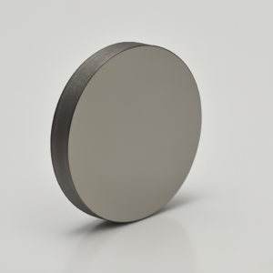
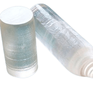
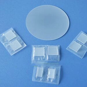
TGG substrates are typically supplied with well-defined crystallographic orientations such as ⟨111⟩ or ⟨100⟩, with single-side or double-side polishing available depending on the application. Surface flatness, parallelism, and roughness are tightly controlled, making these substrates suitable for direct integration into optical assemblies or further coating and bonding processes.
Thanks to their high damage threshold and stable magneto-optical response over a wide temperature range, TGG substrates are particularly well suited for high-power solid-state lasers, industrial laser systems, and scientific research equipment.
Applications
Terbium Gallium Garnet substrates are extensively used in optical, photonic, and laser-based technologies, including:
Faraday rotators for polarization rotation control
Optical isolators in solid-state, fiber, and semiconductor lasers
High-power laser protection systems
Magneto-optical modulators and sensors
Scientific and laboratory optical instruments
Laser systems for industrial, medical, and defense applications
Technical Parameters
| Parameter | Typical Value / Range | Importance |
|---|---|---|
| Material | Terbium Gallium Garnet (Tb₃Ga₅O₁₂) | Core magneto-optical functionality |
| Crystal Structure | Cubic garnet | Ensures isotropic optical behavior |
| Orientation | ⟨111⟩, ⟨100⟩ | Influences optical alignment and performance |
| Transparency Range | 400 – 1600 nm | Covers visible to near-infrared lasers |
| Verdet Constant | ~40 rad/T·m @ 1064 nm | Determines Faraday rotation efficiency |
| Diameter / Size | Custom wafers or substrates | Fits specific optical assemblies |
| Surface Finish | SSP / DSP, optical polish | Impacts scattering and insertion loss |
Comparison with Related Materials
| Material | Key Advantage | Typical Application |
|---|---|---|
| Terbium Gallium Garnet (TGG) | High Verdet constant, high laser damage threshold | Optical isolators, Faraday rotators |
| Yttrium Iron Garnet (YIG) | Strong magneto-optical effect at microwave frequencies | RF & microwave devices |
| Terbium Aluminum Garnet (TAG) | Magneto-optical properties, but less stable | Specialized optical systems |
| Quartz | Excellent optical clarity | Passive optical components |
FAQ
| Question | Answer |
|---|---|
| Can TGG substrates be customized? | Yes, size, thickness, orientation, and polishing can be tailored. |
| Are TGG substrates suitable for high-power lasers? | Yes, they offer high laser damage resistance and thermal stability. |
| What polishing quality is available? | Optical-grade single-side or double-side polishing is available. |
| Which wavelengths are best supported? | Common laser wavelengths from visible to near-infrared, including 532 nm and 1064 nm. |
Packaging
Our Terbium Gallium Garnet Substrate (TGG) products are individually labeled and handled in clean environments to ensure full traceability and surface integrity. Each substrate is securely packaged with protective materials to prevent mechanical damage and contamination during storage and international transportation.
Conclusion
Terbium Gallium Garnet substrates are a cornerstone material for reliable and high-performance magneto-optical devices. Their exceptional Faraday rotation efficiency, optical transparency, and durability make them the preferred choice for optical isolators and high-power laser systems.
For detailed specifications and a quotation, please contact us at sales@thinfilmmaterials.com.
Reviews
There are no reviews yet.