
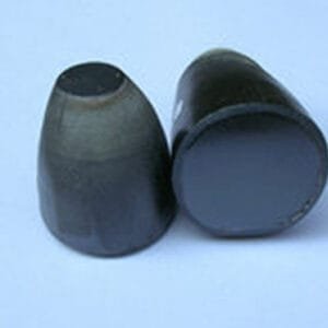
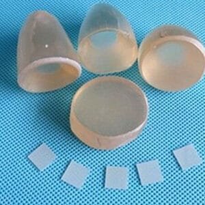
Rutile Substrate (TiO2)
TFM offers high-quality Rutile (TiO₂) substrates, known for their excellent optical, dielectric, and structural properties. These substrates are widely used in thin-film epitaxy, optoelectronic devices, and photonic applications, thanks to their high refractive index, superior transparency, and excellent lattice matching with various functional materials.
Rutile TiO₂ substrates are ideal for oxide thin-film growth, including ferroelectric, multiferroic, and superconducting materials. Their low absorption in the visible and infrared range makes them suitable for optical coatings, waveguides, and high-performance photonic devices. Additionally, the high dielectric constant and thermal stability of TiO₂ support applications in high-frequency and power electronic devices.
TFM supplies precisely engineered Rutile TiO₂ substrates in various orientations and sizes, ensuring optimal performance for advanced material research and next-generation electronic and optical technologies.
Physical Properties
- Material: Rutile (TiO2)
- Crystal Structure: M4
- Lattice Constants:
- a = 4.5936 Å
- c = 2.9582 Å
- Growth Method: Vernuil method, Float zone method
- Hardness: 7.0 on the Mohs scale
- Density: 4.26 g/cm³
- Melting Point: 1870°C
- Dielectric Constants:
- dη/dT: a = -0.72 × 10⁻⁶/K, c = -0.42 × 10⁻⁶/K
- Linear Expansion Coefficients:
- 7.14 × 10⁻⁶/°C along the a-axis
- 9.19 × 10⁻⁶/°C along the c-axis
Specifications
- Size Options:
- 5×5×10mm
- 5×10×10mm
- 10×10×0.5mm
- Custom sizes available upon request
- Polished: SSP or DSP
Packaging
Rutile Substrates are carefully packaged in class 100 clean bags or wafer containers, all within a class 1000 clean room, ensuring protection during handling and transport.
Ideal for optical devices requiring high precision, Rutile Substrates provide an excellent solution for high-performance applications.

Reviews
There are no reviews yet.