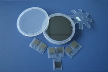
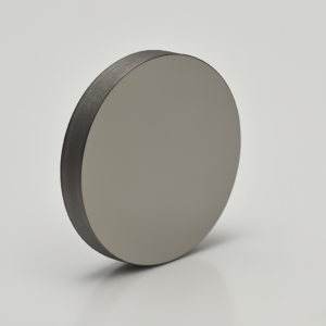
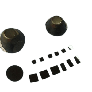
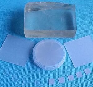
TFM Indium Phosphide Wafer: High Performance, High Precision
TFM provides high-purity Indium Phosphide Wafer (InP), renowned for their exceptional electronic and optoelectronic properties. InP wafers offer high electron mobility, direct bandgap characteristics, and superior thermal conductivity, making them ideal for high-speed, high-frequency, and photonic applications.
InP wafers are extensively used in optoelectronics, fiber-optic communication, and high-frequency RF devices, including laser diodes, photodetectors, and high-speed transistors. Their low lattice mismatch with III-V compound semiconductors ensures excellent epitaxial layer growth, enhancing device performance and efficiency.
TFM supplies InP wafers in various sizes and specifications, tailored to meet the stringent demands of semiconductor research and advanced device fabrication, ensuring optimal performance for next-generation electronic and optical technologies.
Indium Phosphide Wafer Specifications
| Size | 10 x 10 x 0.35mm, 10 x 5 x 0.35mm, 2″ Dia, 3″ Dia, 4″ Dia (custom sizes available) |
|---|---|
| Thickness | 0.35 mm, 0.6 mm |
| Polished | SSP or DSP |
| Orientation | <100>, <111> |
| Redirection Precision | ±0.5° |
| Primary Flat Length | 16±2 mm, 22±2 mm, 32.5±2 mm |
| Secondary Flat Length | 8±1 mm, 11±1 mm, 18±1 mm |
| TTV | <10 µm, <15 µm |
| Bow | <10 µm, <15 µm |
| Warp | <15 µm |
Indium Phosphide Wafer Physical Properties
| Material | InP |
|---|---|
| Growth Method | LEC, VCZ/P-LEC, VGF, VB |
| Lattice (Å) | a = 5.869 |
| Structure | M3 |
| Melting Point | 1600°C |
| Density (g/cm³) | 4.79 g/cm³ |
| Doped Materials | Undoped, S-doped, Zn-doped, Fe-doped |
| Type | N, N, P, N |
| Carrier Concentration (cm⁻³) | (0.4-2) x 10¹⁶, (0.8-3) x 10¹⁸, (4-6) x 10¹⁸, (0.6-2) x 10¹⁸, 10⁷-10⁸ |
| Mobility (cm²/V·s) | (3.5-4) x 10³, (2.2-2.4) x 10³, (1.3-1.6) x 10³, 70-90, ≥2000 |
| EPD (Average) | <5 x 10⁴/cm², 3 x 10⁴/cm², 2 x 10³/cm², 2 x 10⁴/cm², 3 x 10⁴/cm² |


Reviews
There are no reviews yet.