In the dynamic realm of materials science and technology, certain elements emerge as pivotal players, driving innovation and enabling breakthroughs across industries. Germanium, a versatile metalloid, stands out as one such element, playing a critical role in the development of cutting-edge technologies. This comprehensive guide explores the world of Germanium Sputter Targets, shedding light on their significance, applications, and the transformative technologies they enable.
Introduction to Germanium Sputter Targets
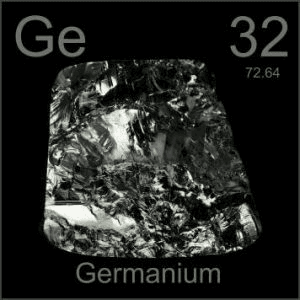
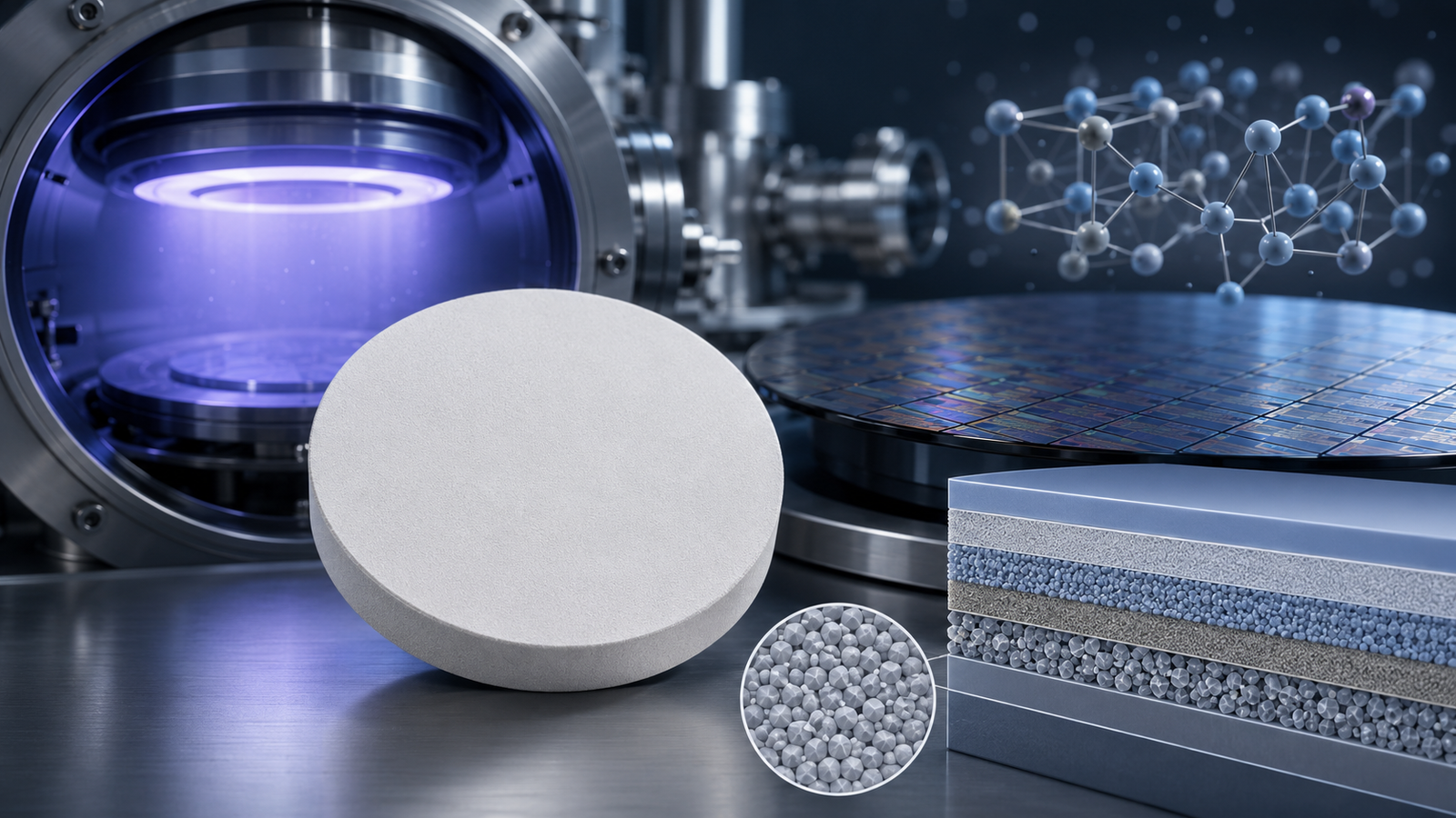
Germanium (Ge), with its atomic number 32, is a metalloid nestled in the carbon group of the periodic table. Known for its lustrous, hard, and grayish-white appearance, germanium shares chemical similarities with silicon and tin, making it a versatile material in electronics, photonics, and beyond. Among its many forms, Germanium Sputter Targets represent a highly refined and pure version of this element, specifically engineered for use in the sputtering process—a cornerstone technique in thin film deposition.
Sputtering is a physical vapor deposition (PVD) method used to create ultra-thin, uniform layers of germanium on various substrates. These layers are essential in the fabrication of semiconductors, optical devices, and solar cells, making germanium sputter targets indispensable in modern manufacturing processes.
A Closer Look at Germanium’s Unique Properties
Germanium’s exceptional properties make it a material of choice for a wide range of high-tech applications. Below, we delve into its semiconductor, optical, and mechanical characteristics, highlighting why it is so highly valued.
1. Semiconductor Excellence
Germanium’s narrow bandgap of approximately 0.66 eV at room temperature sets it apart from other semiconductor materials like silicon. This property allows for efficient movement of charge carriers (electrons and holes), enabling devices to operate at lower voltages and higher speeds. As a result, germanium is widely used in the production of high-speed transistors, integrated circuits, and advanced microelectronics.
2. Optical Properties
One of germanium’s most remarkable features is its transparency to infrared (IR) light, with a transmission range of 2 to 14 µm. This makes it an ideal material for infrared optics, including lenses and windows for thermal imaging cameras, night vision devices, and fiber optic systems. Its ability to modify the refractive index of silica-based fibers also enhances signal transmission in telecommunications.
3. Mechanical and Thermal Characteristics
Germanium exhibits a high melting point of 938°C (1720°F) and excellent thermal conductivity, ensuring stability under extreme thermal conditions. These properties make it suitable for demanding applications in aerospace, military, and high-temperature electronics, where reliability and durability are paramount.
| Property Category | Property | Impact/Application |
|---|---|---|
| Semiconductor Excellence | Bandgap: ~0.66 eV | Enables high-speed, low-voltage operation in transistors and integrated circuits. |
| Optical Properties | Transparency: 2 to 14 µm IR light | Essential for infrared optics, thermal imaging, and fiber optic communication. |
| Mechanical Characteristics | High Melting Point: ~938°C (1720°F) | Ensures stability in high-temperature environments, critical for aerospace and defense. |
| Thermal Characteristics | Good Thermal Conductivity | Maintains performance across a wide temperature range, enhancing device reliability. |
The Essence of Sputtering
Sputtering is a cornerstone of physical vapor deposition (PVD), a process that has revolutionized thin film deposition. This technique involves bombarding a solid target material, such as germanium, with high-energy ions (typically from an inert gas like argon) in a vacuum environment. The collision dislodges atoms from the target, which then deposit onto a substrate, forming a thin, uniform film.
How Sputtering Works
- Vacuum Chamber Setup: The process begins in a high-vacuum chamber, where the germanium target is positioned opposite the substrate.
- Ionization of Gas: An inert gas, such as argon, is introduced and ionized to form a plasma.
- Target Bombardment: Positively charged argon ions are accelerated toward the negatively charged germanium target, ejecting germanium atoms upon impact.
- Film Deposition: The ejected germanium atoms travel through the vacuum and condense onto the substrate, forming a thin film.
This precise and controllable process ensures the creation of high-quality films with exceptional uniformity and adhesion, making sputtering indispensable in industries ranging from electronics to optics.
Diverse Applications of Germanium Sputter Targets
Germanium sputter targets are integral to a multitude of industries, enabling advancements in electronics, optics, and renewable energy. Below, we explore their key applications.
1. Semiconductor Devices
Germanium’s high carrier mobility makes it a preferred material for high-speed transistors, diodes, and integrated circuits. Its compatibility with silicon allows for the creation of heterojunction devices, which enhance the performance of electronic components in smartphones, computers, and other devices.
2. Fiber Optics
Germanium-doped silica is widely used in the core of fiber optic cables, where it modifies the refractive index to enable efficient light transmission. This application is critical for high-speed internet and telecommunications networks, ensuring minimal signal loss over long distances.
3. Infrared Optics
Germanium’s transparency to infrared light makes it indispensable in thermal imaging cameras, night vision devices, and infrared spectroscopy. These technologies are vital for applications in security, surveillance, and medical imaging.
4. Solar Cells
Germanium serves as a substrate for multijunction solar cells, which are used in space applications and concentrated photovoltaic systems. Its ability to absorb a broad spectrum of sunlight significantly enhances the efficiency of solar energy conversion.
Innovations and Future Directions
The field of germanium sputter targets is continually evolving, driven by the need for more efficient, cost-effective, and sustainable manufacturing processes. Key innovations include:
- Germanium Alloy Targets: Incorporating elements like gallium or arsenic to enhance electrical and optical properties.
- Advanced Deposition Techniques: Improving control over film characteristics to create materials with tailored properties.
- Sustainability Efforts: Developing recycling methods to recover germanium from end-of-life products and manufacturing waste.
These advancements promise to unlock new possibilities in electronics, optics, and renewable energy, ensuring germanium’s continued relevance in the tech landscape.
Conclusion
Germanium sputter targets are at the forefront of technological innovation, enabling the creation of high-performance semiconductors, optical devices, and energy-harvesting systems. Their unique properties, combined with the precision of the sputtering process, make them indispensable in modern manufacturing. As research and development efforts continue to push the boundaries of material science, germanium will remain a cornerstone of advanced technologies, driving progress across industries and shaping the future of innovation.