Introduction
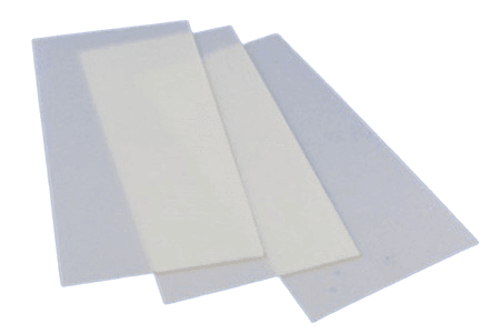
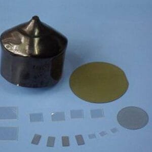
The Zirconia Ceramic Substrate (ZrO₂) is a high-performance ceramic material widely used in electronics, thin film deposition, and high-temperature applications. Known for its exceptional mechanical strength, thermal stability, and chemical resistance, zirconia ceramics are ideal substrates for advanced electronic devices and functional coatings.
Zirconia substrates provide excellent dimensional stability and electrical insulation while maintaining strong resistance to thermal shock and wear. These characteristics make them particularly valuable in semiconductor devices, sensor technologies, fuel cells, and high-temperature electronics. Their compatibility with various thin film deposition methods also makes ZrO₂ substrates suitable for sputtering, evaporation, and other physical vapor deposition processes.
Detailed Description
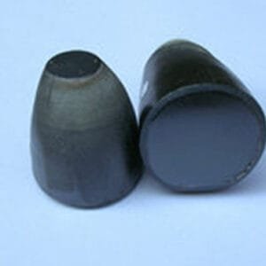
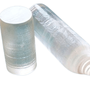
Zirconia ceramic substrates are typically manufactured from high-purity zirconium oxide powders using advanced ceramic processing techniques such as pressing, sintering, and precision machining. In many applications, zirconia is stabilized with additives such as yttria (Y₂O₃) or magnesia (MgO) to improve structural stability and prevent phase transformations at high temperatures.
The stabilized zirconia structure provides outstanding mechanical properties, including high fracture toughness and resistance to crack propagation. Compared with many traditional ceramic substrates, zirconia offers significantly higher strength and durability, making it suitable for demanding environments involving mechanical stress or rapid temperature changes.
Another key advantage of zirconia substrates is their excellent ionic conductivity at elevated temperatures, especially in yttria-stabilized zirconia (YSZ). This property makes them important components in solid oxide fuel cells (SOFCs), oxygen sensors, and other electrochemical devices.
For thin film applications, zirconia substrates provide a stable and chemically inert platform for depositing metal, oxide, and semiconductor films. The smooth and dense surface structure supports uniform film growth and strong adhesion, which is critical for high-performance electronic devices and optical coatings.
Applications
Zirconia ceramic substrates are used in many advanced technology fields, including:
Semiconductor and microelectronic devices requiring stable insulating substrates
Thin film deposition platforms for sputtering and evaporation coatings
Solid oxide fuel cells (SOFCs) and electrochemical devices
Oxygen sensors and gas sensors operating at high temperatures
High-temperature electronic components and insulating layers
Research and development laboratories studying advanced ceramic materials
Technical Parameters
| Parameter | Typical Value / Range | Importance |
|---|---|---|
| Material | Zirconium Oxide (ZrO₂) | Provides high strength and thermal stability |
| Purity | ≥ 99.5% | Ensures consistent ceramic properties |
| Density | ~5.8 – 6.1 g/cm³ | High density improves mechanical durability |
| Surface Finish | Polished or precision ground | Supports high-quality thin film deposition |
| Size | Custom sizes available | Compatible with various device structures |
| Temperature Resistance | Up to ~2400 °C (material stability) | Suitable for extreme environments |
Comparison with Related Materials
| Material | Key Advantage | Typical Application |
|---|---|---|
| Zirconia (ZrO₂) | High fracture toughness and thermal stability | Sensors, fuel cells, and high-temperature electronics |
| Alumina (Al₂O₃) | Excellent electrical insulation and cost-effectiveness | General electronic substrates |
| Sapphire (Al₂O₃ single crystal) | Superior optical clarity and hardness | Optoelectronic and optical devices |
FAQ
| Question | Answer |
|---|---|
| What types of zirconia substrates are available? | Common types include yttria-stabilized zirconia (YSZ), magnesia-stabilized zirconia (MSZ), and partially stabilized zirconia (PSZ). |
| Can zirconia substrates be customized? | Yes. Thickness, dimensions, surface finish, and stabilization type can be customized according to application requirements. |
| Are zirconia substrates suitable for thin film deposition? | Yes. Their dense surface and high thermal stability make them excellent substrates for sputtering and evaporation coatings. |
| What surface finishes are available? | Substrates can be supplied as polished, ground, or lapped surfaces depending on deposition or device requirements. |
| What industries use zirconia ceramic substrates most often? | Semiconductor manufacturing, energy technologies, sensor development, and advanced materials research. |
Packaging
Our Zirconia Ceramic Substrate (ZrO₂) products are meticulously tagged and labeled externally to ensure efficient identification and maintain high standards of quality control. Each substrate is carefully packaged with protective materials, vacuum-sealed bags, and shock-resistant export cartons to prevent contamination and mechanical damage during storage and transportation.
Conclusion
The Zirconia Ceramic Substrate (ZrO₂) provides an excellent combination of mechanical strength, thermal stability, and chemical resistance, making it a reliable platform for advanced electronic devices and thin film technologies. Its superior durability and high-temperature performance distinguish it from many conventional ceramic substrates.
With customizable dimensions, precision surface finishing, and high material purity, zirconia substrates support demanding applications across semiconductor manufacturing, energy technologies, and advanced research.
For detailed specifications and a quotation, please contact us at sales@thinfilmmaterials.com.
Reviews
There are no reviews yet.