“`html
2D Material Sputtering Targets: MoS₂, WS₂, and Beyond
Introduction to 2D Materials and Sputtering
Two-dimensional (2D) materials have revolutionized the landscape of material science due to their atomic-scale thickness and exceptional electronic, optical, and mechanical properties. Since the isolation of graphene, a single layer of carbon atoms, researchers have sought other 2D materials with tunable bandgaps, high carrier mobility, and unique surface chemistry. Among these, transition metal dichalcogenides (TMDs) such as molybdenum disulfide (MoS₂) and tungsten disulfide (WS₂) have gained tremendous attention for applications in electronics, optoelectronics, catalysis, and energy storage.
One of the most effective methods for fabricating thin films of these materials is sputtering—a physical vapor deposition (PVD) technique that enables precise control over film thickness, composition, and uniformity. Sputtering targets composed of 2D materials, or their precursors, are at the heart of this technology. This article explores the science, technology, and applications of 2D material sputtering targets, focusing on MoS₂, WS₂, and exploring the expanding universe of related compounds.
2D Materials: Overview and Significance
What Are 2D Materials?
2D materials are crystalline solids consisting of a single layer or a few atomic layers. Their atomic-scale thickness imparts unique electronic, mechanical, and optical properties not found in their bulk counterparts. The most famous 2D material, graphene, is a single layer of carbon atoms arranged in a hexagonal lattice, renowned for its high electrical conductivity and mechanical strength.
Beyond graphene, the 2D family encompasses a variety of materials including:
- Transition metal dichalcogenides (TMDs): MoS₂, WS₂, MoSe₂, WSe₂, etc.
- Transition metal oxides: TiO₂, MoO₃, etc.
- Hexagonal boron nitride (h-BN)
- Black phosphorus (phosphorene)
- 2D carbides and nitrides (MXenes)
- Metal halides, silicon-based 2D materials, and more
Unique Properties and Applications
2D materials offer:
- Layer-dependent bandgaps (direct/indirect transitions)
- High surface-to-volume ratio
- Excellent mechanical flexibility
- Strong light-matter interaction
- Chemical tunability via doping or functionalization
These features make them ideal for:
- Field-effect transistors (FETs)
- Photodetectors and photovoltaics
- Catalysts (e.g., for hydrogen evolution reactions)
- Flexible electronics and sensors
- Supercapacitors and batteries
Sputtering: A Gateway to Thin Film 2D Materials
Principle of Sputtering
Sputtering is a PVD method where energetic ions (typically Ar⁺) bombard a solid target, ejecting atoms or molecules from its surface. These ejected species travel through a vacuum and condense onto a substrate, forming a thin film. Sputtering allows for fine control over film thickness, composition, and uniformity, making it invaluable for research and industrial production.
Types of Sputtering
- DC Sputtering: For conductive targets (e.g., metals, some TMDs).
- RF Sputtering: For insulating or semiconducting targets (e.g., oxides, sulfides).
- Reactive Sputtering: Adding reactive gases (O₂, S₂, N₂) to form compounds on the substrate.
- Magnetron Sputtering: Uses magnetic fields to confine electrons, increasing ionization and deposition rates.
Why Sputtering for 2D Materials?
- Scalable and compatible with large-area substrates
- Good control over stoichiometry and thickness
- Low substrate temperatures possible
- Integration with existing semiconductor fabrication lines
Sputtering Targets: The Heart of the Process
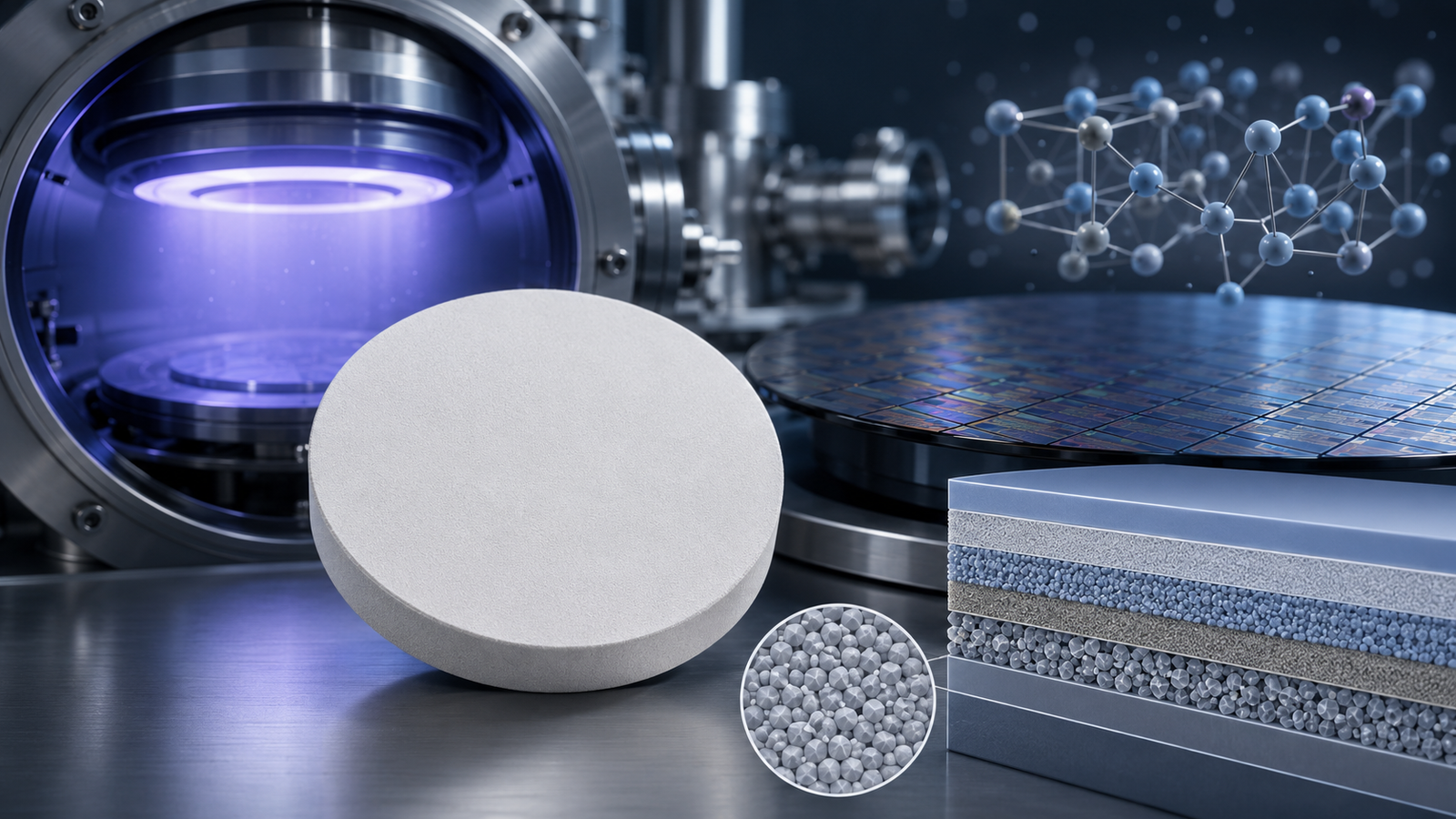
What Are Sputtering Targets?
Sputtering targets are solid materials from which atoms are ejected during the sputtering process. For 2D material fabrication, targets can be:
- Elemental (e.g., Mo, W, S, Se)
- Compound (e.g., MoS₂, WS₂, MoSe₂, MoTe₂, etc.)
- Alloys or composite targets for co-sputtering
The choice of target type affects film growth, composition, and quality.
Forms and Specifications
Targets are manufactured in various shapes and sizes:
- Discs (planar targets)
- Plates
- Columns (cylindrical targets)
- Step targets (with varying thickness)
- Custom shapes for specific equipment
Key specifications include:
- Purity (commonly >99.9% for electronic applications)
- Density (higher density minimizes porosity and improves uniformity)
- Grain size (smaller grains offer better film uniformity)
- Bonding type (Indium, elastomer, etc.)
MoS₂ Sputtering Targets: The Prototypical 2D Material
Material Profile: MoS₂
Molybdenum disulfide (MoS₂) is a TMD with a layered structure, where each layer comprises a plane of Mo atoms sandwiched between two planes of S atoms. Its properties include:
- Bandgap: ~1.2-1.9 eV (layer-dependent, indirect to direct transition)
- Color: Black, crystalline solid
- Melting point: 1,185°C
- Theoretical density: 5.06 g/cm³
Target Production and Forms
MoS₂ sputtering targets are typically produced via hot pressing or cold isostatic pressing followed by sintering. They are available in disc, plate, column, and step target forms, with custom shapes possible.
Common purities exceed 99%, and targets are bonded using indium or elastomeric layers to facilitate heat dissipation and mechanical stability during sputtering.
Deposition and Film Properties
MoS₂ thin films deposited by sputtering exhibit:
- Uniform thickness control
- High adhesion to substrates (Si, glass, sapphire)
- Tunable stoichiometry (via sputtering parameters)
- Layer-by-layer growth possible for few-layer films
Sputtered MoS₂ films are used in:
- Transistors and photodetectors
- Solid lubricants (due to low friction)
- Catalysts for hydrogen evolution
- Flexible electronics
Challenges in Sputtering MoS₂
- Controlling stoichiometry: S loss can occur due to high-vacuum or high-temperature conditions.
- Film crystallinity: Post-deposition annealing may be required to enhance crystallinity and electrical properties.
- Target cracking: Due to brittleness, careful handling and bonding are critical.
WS₂ Sputtering Targets: The Tungsten Counterpart
Material Profile: WS₂
Tungsten disulfide (WS₂) shares a similar layered structure with MoS₂, but with W atoms between S planes. Its properties include:
- Bandgap: ~1.3-2.1 eV (layer-dependent)
- High chemical and thermal stability
- Excellent lubricating properties
- Color: Dark gray to black
- Melting point: ~1,250°C
- Theoretical density: ~7.5 g/cm³
Target Specifications
WS₂ targets are produced with similar techniques as MoS₂, with high purity (>99%), and are available in a variety of shapes and sizes.
Deposition and Applications
Sputtered WS₂ thin films are used in:
- Electronic and optoelectronic devices (transistors, photodetectors)
- Solid lubrication, especially in extreme environments
- Catalytic applications
- Protective coatings
WS₂ films benefit from higher thermal stability and chemical resistance compared to MoS₂, making them suitable for harsh environments.
Beyond MoS₂ and WS₂: The Expanding Frontier
Other Transition Metal Dichalcogenide (TMD) Targets
The family of TMDs extends beyond MoS₂ and WS₂ to include a variety of transition metal chalcogenides with tailored properties:
- Molybdenum Selenide (MoSe₂): Lower bandgap, used in photovoltaic and optoelectronic devices.
- Molybdenum Telluride (MoTe₂): Narrow bandgap, phase-change properties, and potential for topological electronics.
- Tungsten Selenide (WSe₂): Strong spin-orbit coupling, valleytronics applications.
- Molybdenum Boride (Mo₂B₅): Hard, wear-resistant coatings.
- Silicon Sulfide (SiS₂): 2D analogs under investigation for electronics and sensors.
Target Production and Customization
These targets are manufactured to high purity standards (up to 99.999%) and are available in discs, plates, columns, and custom geometries. Target bonding options (indium, elastomer) are selected based on thermal and mechanical requirements.
Alloy and Compound Targets
Co-sputtering from multiple targets (e.g., Mo and S) or using alloy/composite targets (e.g., Mo/W) enables the fabrication of tailored 2D films with specific stoichiometry, strain, or doping profiles. This is essential for research into heterostructures, bandgap engineering, and novel functionalities.
Advances in Sputtering Techniques for 2D Films
Reactive Sputtering
Reactive sputtering involves introducing reactive gases (such as H₂S or Se vapor) into the chamber during sputtering from a pure metal target (e.g., Mo or W), enabling the in-situ formation of chalcogenides on the substrate. This offers flexibility in tuning film composition and properties.
Co-Sputtering and Layered Heterostructures
Co-sputtering from two or more targets allows for the creation of:
- Alloyed 2D materials (e.g., MoₓW₁₋ₓS₂)
- Vertical/lateral heterostructures (e.g., MoS₂-WS₂ junctions)
- Doped 2D films (e.g., Nb-doped MoS₂ for enhanced conductivity)
Such heterostructures are crucial for next-generation electronic and optoelectronic devices.
Pulsed Laser Deposition (PLD) and Hybrid Methods
While sputtering is dominant, hybrid methods such as pulsed laser deposition (PLD) using bulk TMD targets can also produce high-quality 2D films. Combining sputtering with post-deposition annealing or chalcogenization steps further improves film crystallinity and properties.
Substrate Considerations
The choice of substrate (Si, SiO₂, sapphire, glass, flexible polymers) influences film growth, morphology, and properties. Sputtering parameters must be optimized for each substrate type to achieve desired film characteristics.
Characterization of Sputtered 2D Films
Structural Characterization
- Raman spectroscopy: Layer count, crystallinity, phase
- X-ray diffraction (XRD): Crystalline structure, orientation
- Transmission electron microscopy (TEM): Atomic-scale structure
- Atomic force microscopy (AFM): Surface roughness, thickness
Compositional and Chemical Analysis
- X-ray photoelectron spectroscopy (XPS): Stoichiometry, oxidation states
- Energy dispersive X-ray spectroscopy (EDS): Elemental mapping
Electrical and Optical Measurements
- Hall effect measurements: Carrier type and mobility
- Photoluminescence (PL): Bandgap, defects
- UV-Vis absorption: Optical properties
Applications of 2D Material Thin Films
Electronics and Semiconductors
Sputtered MoS₂, WS₂, and related films are being developed for:
- Field-effect transistors (FETs) with high on/off ratios
- Flexible and transparent electronics
- Logic circuits
Optoelectronics
The strong light-matter interaction and tunable bandgaps of 2D materials make them ideal for:
- Photodetectors
- Light-emitting diodes (LEDs)
- Solar cells (as absorber or buffer layers)
Energy Storage and Conversion
2D TMD films are promising for:
- Electrocatalysts for hydrogen evolution reaction (HER)
- Supercapacitor electrodes
- Lithium/sodium-ion battery anodes
Lubrication and Protective Coatings
The lamellar structure of MoS₂ and WS₂ enables ultra-low friction and high wear resistance, making sputtered films attractive for:
- Microelectromechanical systems (MEMS) lubricants
- Protective coatings for cutting tools and machine parts
- Automotive and aerospace applications
Sensors and Catalysis
High surface area and tunable electronic properties make sputtered 2D TMD films suitable for:
- Chemical and biological sensors
- Environmental monitoring devices
- Photocatalysis
Comparison of Sputtering Targets: MoS₂, WS₂, and Others
| Material | Formula | Purity (%) | Melting Point (°C) | Density (g/cm³) | Color/Appearance | Bonding Type | Applications |
|---|---|---|---|---|---|---|---|
| Molybdenum Disulfide | MoS₂ | >99.0 | 1,185 | 5.06 | Black, crystalline | Indium, Elastomer | Electronics, Lubrication, Catalysis |
| Tungsten Disulfide | WS₂ | >99.0 | ~1,250 | 7.5 | Dark gray, black | Indium, Elastomer | Optoelectronics, Lubrication, Catalysis |
| Molybdenum Selenide | MoSe₂ | 99.9-99.999 | ~1,200 | 6.5 | Black, crystalline | Indium, Elastomer | Photovoltaics, Electronics |
| Molybdenum Telluride | MoTe₂ | 99.9-99.999 | ~1,250 | 7.8 | Black, crystalline | Indium, Elastomer | Phase-change, Topological electronics |
| Silicon Sulfide | SiS₂ | >99.0 | 1,090 | 1.85 | White, solid | Indium, Elastomer | Electronics, Sensors |
Target Bonding and Handling
Sputtering targets, especially those composed of brittle or thermally sensitive materials like MoS₂, WS₂, and their analogs, are often bonded to a backing plate (usually copper or stainless steel) using indium or elastomer layers. This ensures:
- Efficient heat transfer during sputtering
- Minimized risk of cracking or delamination
- Improved mechanical stability
Careful degassing and handling are essential to prevent contamination and damage.
Manufacturing and Customization of Sputtering Targets
Production Techniques
- Powder metallurgy: Mixing, pressing, and sintering high-purity powders.
- Hot pressing: Applies heat and pressure to densify powders.
- Chemical vapor deposition (CVD): For some high-purity targets.
- Machining: Cutting and shaping into discs, plates, or custom geometries.
Customization Options
Manufacturers offer a range of options:
- Diameters: 1.0″, 2.0″, 3.0″, 4.0″, 5.0″, 6.0″ and larger
- Thicknesses: 0.125″, 0.250″, or custom
- Purity levels: 99.9%, 99.95%, 99.99%, 99.995%, 99.999%
- Custom shapes: Step targets, rectangular, annular, etc.
Quality Control and Certification
Stringent quality control ensures:
- Consistent composition and stoichiometry
- Minimal impurities and contamination
- Uniform density and grain size
- Certification (COA, RoHS, REACH compliance)
Case Study: Molybdenum Disulfide Sputtering Target (MoS₂)
Specifications and Forms
- Chemical Formula: MoS₂
- Catalog Number: ST0284
- CAS Number: 1317-33-5
- Purity: >99%
- Available Shapes: Discs, Plates, Column Targets, Step Targets, Custom-made
Key Properties
- Color/Appearance: Black, Crystalline Solid
- Melting Point: 1,185°C
- Theoretical Density: 5.06 g/cm³
- Sputtering Type: RF
- Bonding: Indium, Elastomer
Applications
- Field-effect transistors (FETs)
- Optoelectronic devices
- Solid lubricants
- Hydrogen evolution catalysts
Process Notes
- Careful degassing is required to remove adsorbed moisture and gases.
- Indium bonding enhances heat dissipation during high-power sputtering.
- High purity and density improve film uniformity and electronic properties.
Trends and Future Directions in 2D Material Sputtering
Emerging Materials and Heterostructures
The field is rapidly evolving with the exploration of new 2D materials:
- Janus TMDs: Asymmetrically functionalized materials (e.g., MoSSe)
- 2D oxides, nitrides, and carbides (MXenes)
- Vertical and lateral heterostructures for multifunctional devices
- Topological insulators and Weyl semimetals in 2D form
Scalability and Industrial Applications
Sputtering is increasingly adopted for large-area and industrial-scale production of 2D material films, enabling:
- Roll-to-roll processing for flexible electronics
- Integration with CMOS fabrication lines
- Automated quality control and real-time monitoring
Environmental and Safety Considerations
- Minimizing hazardous waste (e.g., chalcogen vapors)
- Recycling and reprocessing spent targets
- Safe handling and disposal of toxic elements (Se, Te)
Conclusion
2D material sputtering targets, especially those based on MoS₂, WS₂, and related compounds, are fundamental to the fabrication of advanced thin films with exceptional properties. Sputtering offers scalable, reproducible, and high-quality deposition of these materials, enabling breakthroughs in electronics, optoelectronics, catalysis, and beyond.
As the library of 2D materials expands and sputtering technology advances, the future holds promise for novel devices and applications built on the unique capabilities of atomically thin films. From customizing target compositions to developing heterostructures and embracing industrial-scale production, the synergy between material innovation and deposition technology will continue to drive the field forward.
References
- Chhowalla, M., et al. “The chemistry of two-dimensional layered transition metal dichalcogenide nanosheets.” Nature Chemistry, 2013.
- Wang, Q.H., et al. “Electronics and optoelectronics of two-dimensional transition metal dichalcogenides.” Nature Nanotechnology, 2012.
- Thin Film Materials Product Catalogs, 2024.
- Scholarly reviews and technical datasheets on MoS₂, WS₂, MoSe₂, and related sputtering targets.
“`