Introduction
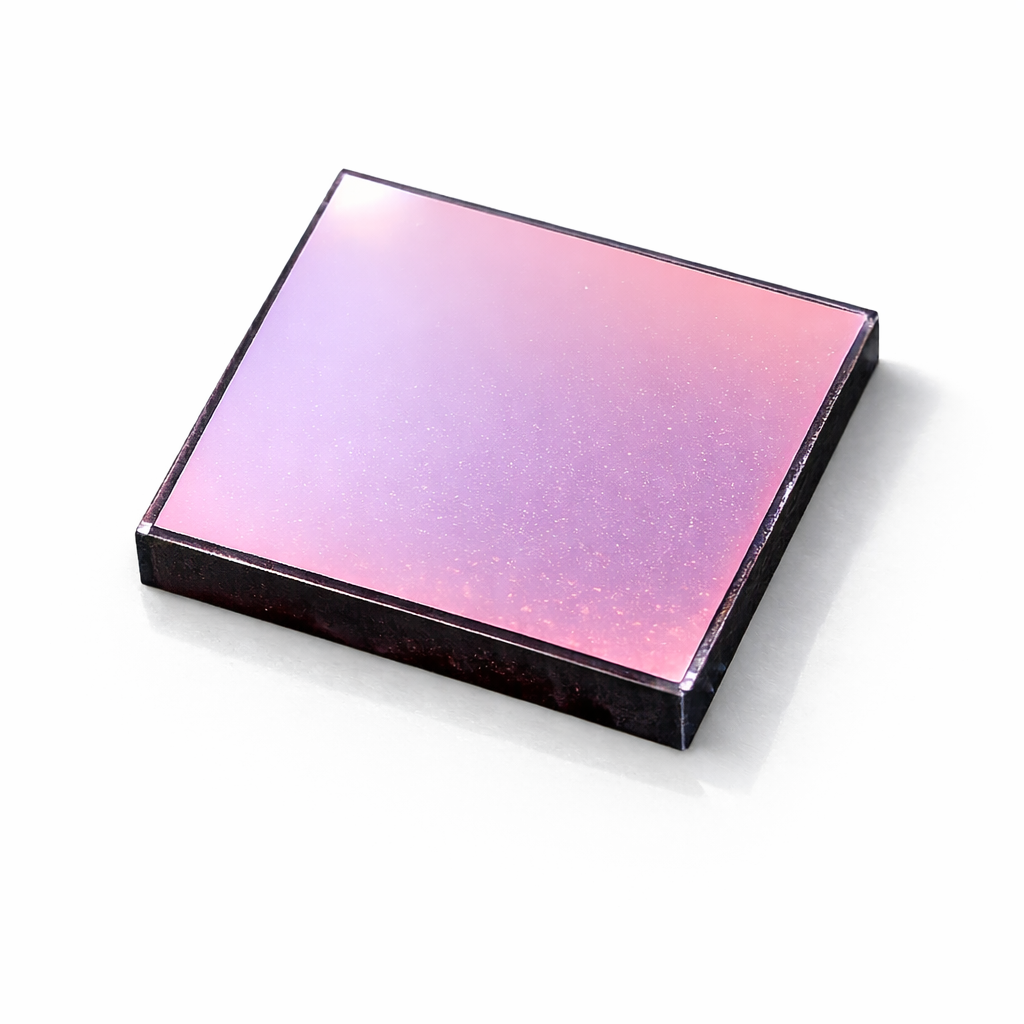
Chromium-Doped Strontium Titanate (Cr:SrTiO₃) Substrate is a functional perovskite oxide crystal widely used in advanced thin film research and oxide electronics. By introducing controlled chromium dopants into the SrTiO₃ lattice, the electrical conductivity and defect chemistry of the crystal can be precisely tailored. This makes Cr:SrTiO₃ substrates particularly valuable for epitaxial growth of complex oxide thin films, resistive switching devices, and high-temperature electronic components.
For researchers working in oxide heterostructures, spintronics, or memristive materials, Cr-doped SrTiO₃ offers a stable and tunable platform with well-defined crystallographic orientation and excellent surface quality.
Detailed Description
Cr:SrTiO₃ is derived from high-purity Strontium Titanate (SrTiO₃) single crystals with chromium ions partially substituting titanium sites within the perovskite structure. The doping level is typically controlled within a narrow molar range (e.g., 0.05–1 at%), depending on the desired electrical behavior.
The introduction of chromium modifies the carrier concentration and introduces deep-level defect states, which significantly influence:
Electrical conductivity and resistivity
Redox stability
Oxygen vacancy dynamics
Resistive switching characteristics
Single-crystal substrates are grown using advanced crystal growth techniques such as the Verneuil or floating zone method, ensuring high structural integrity and minimal dislocation density. After growth, wafers are precisely oriented (e.g., (100), (110), or (111)), sliced, and double-side polished to achieve atomically smooth surfaces suitable for epitaxial deposition.
Surface finishing typically achieves:
Ra < 0.5 nm (epi-polished)
Strict orientation tolerance (±0.5° or better)
Low miscut angle options upon request
Compared with undoped SrTiO₃, chromium doping enhances the substrate’s semiconducting behavior while maintaining lattice compatibility with a wide range of functional oxides, including manganites, ferrites, and high-k dielectric materials.
Applications
Cr:SrTiO₃ substrates are widely used in both academic research and industrial R&D, particularly in:
Resistive switching and memristor devices
Oxide electronics and correlated electron systems
Spintronic heterostructures
Pulsed Laser Deposition (PLD) thin film growth
Magnetoresistive and ferroelectric thin films
Solid oxide fuel cell (SOFC) related research
High-temperature sensor development
Their stable perovskite structure and tunable conductivity make them especially suitable for studying interface-driven phenomena in oxide multilayers.
Technical Parameters
| Parameter | Typical Value / Range | Importance |
|---|---|---|
| Chemical Formula | SrTiO₃:Cr | Controlled doping modifies conductivity |
| Cr Doping Level | 0.05 – 1 at% (customizable) | Determines electrical properties |
| Crystal Orientation | (100), (110), (111) | Affects epitaxial film growth |
| Diameter | 5 – 50 mm | Compatible with common deposition systems |
| Thickness | 0.5 – 1.0 mm (custom) | Mechanical stability during processing |
| Surface Finish | Single-side / Double-side polished | Enables high-quality epitaxy |
| Surface Roughness (Ra) | < 0.5 nm | Critical for thin film uniformity |
Comparison with Related Materials
| Material | Key Advantage | Typical Application |
|---|---|---|
| Chromium-Doped SrTiO₃ | Tunable semiconducting behavior | Resistive switching devices |
| Undoped SrTiO₃ | High dielectric constant, insulating | Epitaxial oxide growth |
| Nb-Doped SrTiO₃ | n-type conductivity | Transparent electrodes |
| LaAlO₃ | Lattice match for specific perovskites | High-mobility oxide interfaces |
Cr doping offers a balance between conductivity and structural compatibility, making it highly versatile in oxide electronics research.
FAQ
| Question | Answer |
|---|---|
| Can the Cr doping concentration be customized? | Yes, doping levels can be precisely controlled according to experimental requirements. |
| What surface orientations are available? | Standard orientations include (100), (110), and (111); other orientations can be provided upon request. |
| Is epi-polished surface available? | Yes, atomically smooth epi-ready surfaces are available for thin film deposition. |
| Are small research-size wafers supported? | Yes, small diameters for laboratory research are available. |
| How are substrates packaged? | Individually packed in cleanroom-grade containers with vacuum-sealed protection. |
Packaging
Our Chromium-Doped Strontium Titanate (Cr:SrTiO₃) Substrates are meticulously tagged and labeled externally to ensure efficient identification and maintain high standards of quality control. We take great care to prevent any potential damage during storage and transportation, ensuring the substrates arrive in perfect condition.
Conclusion
Chromium-Doped Strontium Titanate (Cr:SrTiO₃) Substrate provides a reliable and tunable platform for advanced oxide thin film research and electronic device development. With precise doping control, excellent crystallographic quality, and customizable dimensions, it supports both fundamental studies and applied R&D.
For detailed specifications and a quotation, please contact us at sales@thinfilmmaterials.com.


Reviews
There are no reviews yet.