Introduction
Gadolinium Scandate (GdScO₃) Single Crystal Substrate is an orthorhombic perovskite oxide substrate widely used for epitaxial growth of advanced functional thin films. With its favorable pseudo-cubic lattice parameters and excellent thermal stability, GdScO₃ provides a powerful platform for strain engineering in complex oxide heterostructures.
Due to its strong lattice compatibility with many ABO₃ perovskite oxides, GdScO₃ substrates are particularly valuable in ferroelectric, multiferroic, superconducting, and correlated electron material research.
Detailed Description
Gadolinium Scandate (GdScO₃) crystallizes in a distorted perovskite structure with orthorhombic symmetry. Its pseudo-cubic lattice constant (~3.96–3.97 Å) enables controlled tensile or compressive strain when growing thin films such as BaTiO₃, PbTiO₃, BiFeO₃, and La₁₋ₓSrₓMnO₃.
Key material features include:
Orthorhombic perovskite crystal structure
Excellent lattice match for perovskite thin films
High crystalline uniformity and low defect density
Strong thermal stability during high-temperature deposition (>800°C)
Good chemical stability in typical oxide processing environments
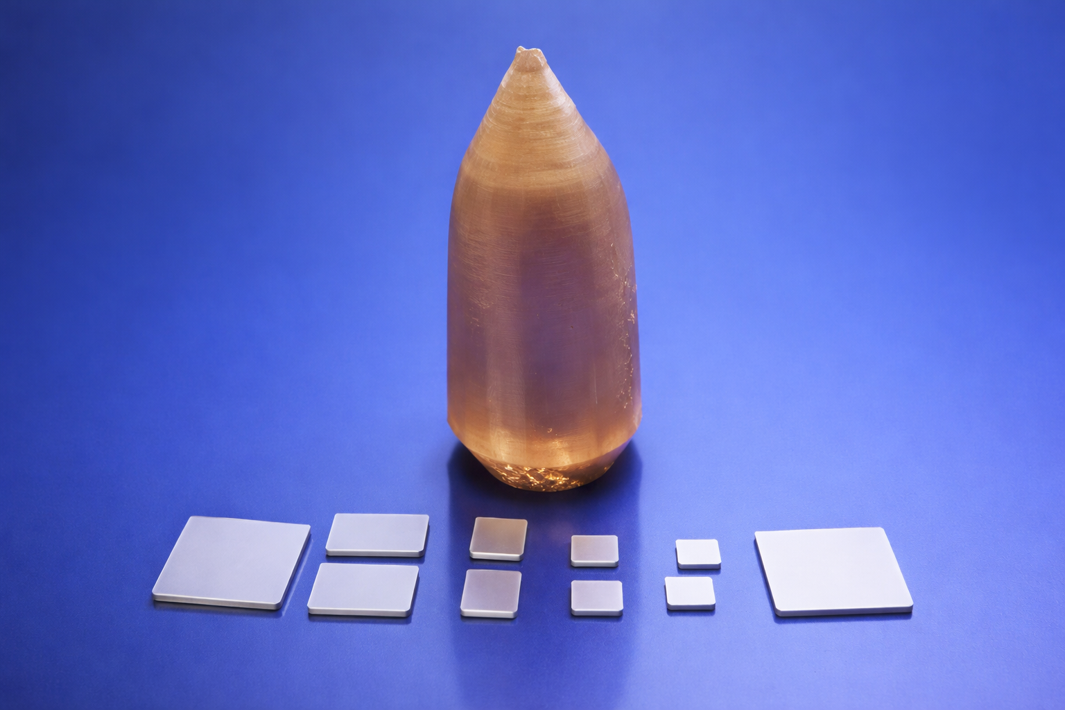
Substrates are grown using precision crystal growth techniques to ensure structural homogeneity. After slicing, wafers undergo chemo-mechanical polishing to achieve epi-ready surfaces with ultra-low roughness. Optional annealing treatment can generate atomically flat step-terrace morphology for high-quality epitaxial growth.
Available orientations commonly include (110), (001), and (101), depending on the strain state and thin film application requirements.
Applications
GdScO₃ Single Crystal Substrate is widely used in:
Ferroelectric thin films (BaTiO₃, PbTiO₃)
Multiferroic materials (BiFeO₃)
Strain-engineered oxide heterostructures
High-mobility perovskite oxide systems
Superconducting thin films
Spintronic and magnetic oxide devices
Advanced sensor and MEMS research
Its strain-inducing capability enables stabilization of novel crystal phases and enhancement of functional properties in oxide films.
Technical Parameters
| Parameter | Typical Value / Range | Importance |
|---|---|---|
| Chemical Formula | GdScO₃ | Defines perovskite structure |
| Crystal Structure | Orthorhombic Perovskite | Enables strain engineering |
| Orientation | (110), (001), (101) | Controls film growth mode |
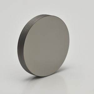
| Surface Finish | SSP / DSP (Epi-ready optional) | Influences epitaxial quality |
| Surface Roughness | < 0.5 nm (epi-ready) | Ensures uniform film growth |
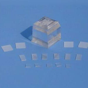
| Size | 5×5 mm – 20×20 mm (custom) | Matches deposition systems |
| Thickness | 0.5 mm – 1.0 mm | Mechanical stability |
| Thermal Stability | Suitable for >800°C deposition | Compatible with oxide growth |
Comparison with Related Materials
| Material | Key Advantage | Typical Application |
|---|---|---|
| GdScO₃ | Strong strain engineering capability | Ferroelectric & multiferroic films |
| DyScO₃ | Similar lattice tuning capability | High-performance oxide films |
| SrTiO₃ | Standard cubic substrate | General oxide epitaxy |
| LaAlO₃ | Good lattice match for selected systems | Interface conductivity studies |
Compared with SrTiO₃, GdScO₃ provides stronger anisotropic strain effects. Compared with LaAlO₃, it typically avoids twin-related structural complications in certain film systems.
FAQ
| Question | Answer |
|---|---|
| Why choose GdScO₃ over SrTiO₃? | GdScO₃ enables enhanced strain engineering and improved phase stabilization for certain perovskite films. |
| Are multiple orientations available? | Yes, common orientations include (110), (001), and (101), with customization available. |
| Is it suitable for high-temperature deposition? | Yes, it maintains structural stability at typical oxide thin film growth temperatures. |
| Can epi-ready surfaces be supplied? | Yes, substrates can be provided with ultra-smooth, atomically flat surfaces. |
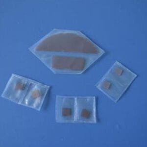
| How is it packaged? | Each substrate is individually protected in clean, vacuum-compatible packaging to prevent contamination and mechanical damage. |
Packaging
Our Gadolinium Scandate (GdScO₃) Single Crystal Substrates are meticulously tagged and labeled externally to ensure efficient identification and maintain high standards of quality control. Special care is taken to prevent surface damage and contamination during storage and transportation.
Conclusion
Gadolinium Scandate (GdScO₃) Single Crystal Substrate offers a high-quality, strain-engineered platform for advanced oxide thin film research and device development. With customizable orientations, excellent thermal stability, and epi-ready surface preparation, GdScO₃ supports cutting-edge applications in ferroelectricity, spintronics, and correlated electron systems.
For detailed specifications and a quotation, please contact us at sales@thinfilmmaterials.com.
Reviews
There are no reviews yet.