单晶基片.png)
Introduction
Terbium Scandate (TbScO₃) Single Crystal Substrate is a high-quality orthorhombic perovskite oxide substrate widely used for epitaxial growth of complex oxide thin films. As part of the rare-earth scandate (REScO₃) family, TbScO₃ offers excellent lattice compatibility with many functional perovskite materials and is particularly valued in strain-engineered thin film research.
With its well-defined pseudo-cubic lattice parameter and strong anisotropic strain capability, TbScO₃ substrates are frequently employed in advanced ferroelectric, multiferroic, and correlated electron systems.
Detailed Description
Terbium Scandate (TbScO₃) crystallizes in an orthorhombically distorted perovskite structure. Its pseudo-cubic lattice constant (~3.95–3.97 Å) provides an effective platform for imposing tensile or compressive strain on epitaxial oxide films.
Key material characteristics include:
Orthorhombic perovskite crystal structure
Strong anisotropic strain engineering capability
High crystalline uniformity and low defect density
Excellent thermal stability during high-temperature deposition (>800°C)
Good chemical stability under standard oxide processing conditions
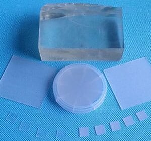
TbScO₃ substrates are grown using advanced crystal growth techniques to ensure structural homogeneity and minimal lattice defects. After slicing, wafers undergo precision chemo-mechanical polishing to achieve atomically smooth surfaces suitable for high-quality epitaxy. Epi-ready surface preparation is available for demanding research applications.
Common orientations include:
(110) — widely used for strain engineering
(001)
(101)
Orientation selection significantly influences domain structure, polarization behavior, and magnetic coupling in deposited films.
Applications
Terbium Scandate (TbScO₃) Single Crystal Substrate is widely used in:
Ferroelectric thin films (BaTiO₃, PbTiO₃)
Multiferroic materials (BiFeO₃)
Strain-engineered perovskite oxide heterostructures
Spintronic and magnetic oxide devices
Correlated electron systems
Superconducting thin film research
Advanced MEMS and sensor materials
Its ability to introduce controlled anisotropic strain enables stabilization of novel structural phases and enhancement of functional properties in oxide thin films.
Technical Parameters
| Parameter | Typical Value / Range | Importance |
|---|---|---|
| Chemical Formula | TbScO₃ | Defines perovskite structure |
| Crystal Structure | Orthorhombic Perovskite | Enables anisotropic strain |
| Orientation | (110), (001), (101) | Controls epitaxial behavior |
| Surface Finish | SSP / DSP (Epi-ready optional) | Influences film quality |
| Surface Roughness | < 0.5 nm (epi-ready) | Ensures uniform growth |
| Size | 5×5 mm – 20×20 mm (custom) | Compatible with deposition systems |
| Thickness | 0.5 mm – 1.0 mm | Mechanical stability |
| Thermal Stability | Suitable for >800°C deposition | High-temperature processing |
Comparison with Related Materials
| Material | Key Advantage | Typical Application |
|---|---|---|
| TbScO₃ | Strong anisotropic strain control | Ferroelectric & multiferroic films |
| DyScO₃ | Similar lattice tuning capability | High-performance oxide films |
| GdScO₃ | Excellent strain engineering | Polarization enhancement studies |
| SrTiO₃ | Standard cubic template | General oxide epitaxy |
Compared with SrTiO₃, TbScO₃ provides stronger anisotropic strain effects. Compared with DyScO₃ and GdScO₃, it offers slightly different lattice parameters, allowing fine tuning of epitaxial strain conditions.
FAQ
| Question | Answer |
|---|---|
| Why choose TbScO₃ over SrTiO₃? | TbScO₃ enables stronger and anisotropic strain engineering for advanced oxide films. |
| Are multiple orientations available? | Yes, standard orientations include (110), (001), and (101). |
| Is it suitable for high-temperature deposition? | Yes, it maintains structural integrity during high-temperature oxide film growth. |
| Can epi-ready surfaces be supplied? | Yes, atomically smooth surfaces are available for demanding epitaxial applications. |
| How is it packaged? | Each substrate is individually protected in clean, vacuum-compatible packaging to prevent contamination and surface damage. |
Packaging
Our Terbium Scandate (TbScO₃) Single Crystal Substrates are meticulously tagged and labeled externally to ensure efficient identification and maintain high standards of quality control. Special care is taken to protect the polished surfaces during storage and transportation, ensuring optimal condition upon delivery.
Conclusion
Terbium Scandate (TbScO₃) Single Crystal Substrate provides a reliable and high-quality platform for strain-engineered oxide thin film research and advanced electronic materials development. With customizable orientations, superior crystalline quality, and epi-ready surface preparation, TbScO₃ supports cutting-edge applications in ferroelectricity, magnetoelectric coupling, and correlated electron systems.
For detailed specifications and a quotation, please contact us at sales@thinfilmmaterials.com.

Reviews
There are no reviews yet.