
P-type Silicon Sputtering Target Description
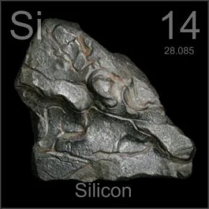 The P-type silicon sputtering target is dark gray with a bluish tinge. Silicon, symbolized as “Si,” derives its name from the Latin word ‘silex’ or ‘silicis,’ meaning flint. It was first mentioned in 1824 and discovered by J. Berzelius, who also accomplished its isolation. Silicon has an atomic number of 14 and is located in Period 3, Group 14 of the periodic table, within the p-block. Its relative atomic mass is 28.0855 Daltons, with the number in brackets indicating the measurement uncertainty.
P-type Silicon Sputtering Target Specification
| Atomic Weight | 28.0855 |
| Atomic Number | 14 |
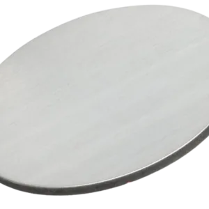
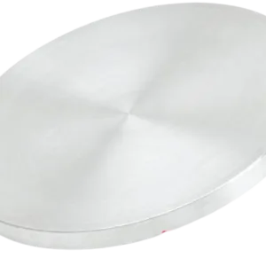
| Color/Appearance | Dark Gray with a Bluish Tinge, Semi-Metallic |
| Thermal Conductivity | 150 W/m.K |
| Melting Point | 1,410 °C |
| Bulk Resistivity | 0.005-0.020 OHM-CM |
| Coefficient of Thermal Expansion | 2.6 x 10⁻⁶/K |
| Theoretical Density | 2.32 g/cc |
| Dopant | Boron |
| Z Ratio | 0.712 |
| Sputter | DC, RF |
| Max Power Density* | 40 Watts/Square Inch |
| Type of Bond | Indium |
P-type Silicon Sputtering Target Handling Notes
- Indium Bonding Recommended: Indium bonding is recommended for P-type silicon sputtering targets due to their brittleness and low thermal conductivity, which are not amenable to sputtering.
- Thermal Conductivity and Shock: P-type silicon has low thermal conductivity and is susceptible to thermal shock, making careful handling and appropriate bonding methods essential.
P-type Silicon Sputtering Target Application
The P-type silicon sputtering target is used in various applications, including:
- Thin film deposition
- Decoration
- Semiconductor manufacturing
- Displays
- LED and photovoltaic devices
- Functional coatings
- Optical information storage
- Glass coating for automotive and architectural glass
- Optical communications
Other Applications of Silicon
- Solar Cells: Silicon is a fundamental material in the production of solar cells.
- Transistors: Essential for manufacturing transistors.
- Semiconductors: Widely used in semiconductor devices.
- Rectifiers and Solid-State Devices: Crucial for various electronics and space sector applications.
P-type Silicon Sputtering Target Packaging
Get Contact
TFM offers P-type silicon Sputtering Targets in various forms, purities, sizes, and prices. We specialize in high-purity thin film deposition materials with optimal density and minimal grain sizes, which are ideal for semiconductor, CVD, and PVD applications in display and optics. Contact Us for current pricing on sputtering targets and other deposition materials that are not listed.

Reviews
There are no reviews yet.