Bismuth Sulfide Sputtering Target
Introduction
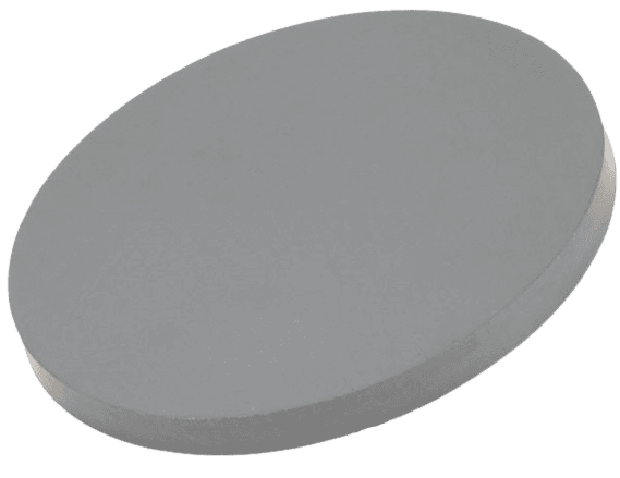
The Bismuth Sulfide (Bi₂S₃) Sputtering Target is a compound target material widely used in thin film deposition. Known for its semiconducting and thermoelectric properties, Bi₂S₃ is a promising material for next-generation optoelectronic devices, infrared sensors, and energy conversion technologies. Its ability to form stable thin films with controlled composition makes it an essential choice for both research laboratories and industrial applications.
Detailed Description
Bismuth Sulfide sputtering targets are manufactured from high-purity Bi₂S₃ powders (≥99.9%) using sintering or hot-pressing techniques. These processes ensure:
High Purity and Low Contamination: Critical for electronic and optical thin film applications.
Uniform Density: Enhances sputtering efficiency and film uniformity.
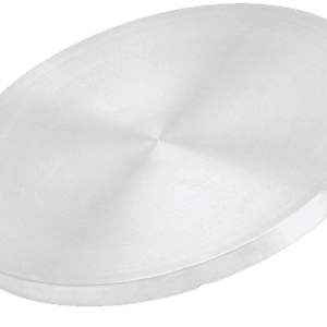
Custom Dimensions: Targets available from 25 mm to 300 mm in diameter, with thicknesses between 3 mm and 6 mm.
Bonding Options: Indium, copper, or elastomer bonding improves heat transfer and mechanical stability during sputtering.
Bismuth Sulfide has an orthorhombic crystal structure, a narrow band gap (~1.3 eV), and excellent photoresponse characteristics, making it highly suitable for infrared optoelectronics and photovoltaics.
Applications
Bismuth Sulfide sputtering targets are used in a wide range of applications, including:
Optoelectronics: Thin films for photodetectors and IR sensors.
Semiconductors: Functional layers in microelectronics and electronic devices.
Solar cells: Absorber layers in thin film photovoltaic devices.
Thermoelectrics: Thin films for energy conversion systems.
Research & Development: Advanced material studies and device prototyping.
Technical Parameters
| Parameter | Typical Value / Range | Importance |
|---|---|---|
| Purity | ≥99.9% (3N) | Ensures low contamination in thin films |
| Diameter | 25 – 300 mm (custom) | Fits a wide range of sputtering systems |
| Thickness | 3 – 6 mm | Influences deposition rate and target lifetime |
| Density | ~6.8 g/cm³ | Supports stable sputtering behavior |
| Bonding | Indium, Copper, Elastomer | Improves thermal conductivity and target stability |
Comparison with Related Materials
| Material | Key Advantage | Typical Application |
|---|---|---|
| Bismuth Sulfide | Narrow bandgap, IR sensitivity | Optoelectronics, photovoltaics |
| Bismuth Oxide (Bi₂O₃) | High ionic conductivity | Solid electrolytes, sensors |
| Zinc Sulfide (ZnS) | Wide bandgap, optical clarity | Optics, protective coatings |
FAQ
| Question | Answer |
|---|---|
| Can Bi₂S₃ sputtering targets be customized? | Yes, dimensions, bonding type, and purity can be tailored. |
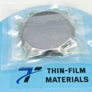
| How are the targets packaged? | Each target is vacuum-sealed, cushioned with protective foam, and packed in export-safe cartons or wooden crates. |
| What industries use Bi₂S₃ targets? | Semiconductor, optics, solar energy, and advanced R&D. |
| Do you supply bonded targets? | Yes, bonding with indium, copper, or elastomer is available for enhanced performance. |
Packaging
Our Bismuth Sulfide sputtering targets are vacuum-sealed to prevent contamination and moisture absorption. Each target is carefully labeled and packed in sturdy cartons or wooden crates, ensuring safe global shipment.
Conclusion
The Bismuth Sulfide (Bi₂S₃) Sputtering Target is a versatile compound target with excellent optoelectronic and thermoelectric properties. With customizable purity, sizes, and bonding options, it provides reliable performance for thin film deposition in photovoltaics, infrared devices, and semiconductor research.
For detailed specifications and a quotation, please contact us at [sales@thinfilmmaterials.com].

Reviews
There are no reviews yet.