Introduction
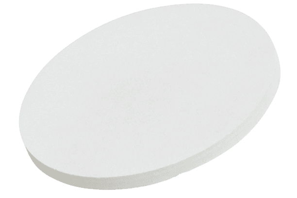
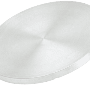
Zinc Sulfide (ZnS) Sputtering Target is a compound ceramic target widely used for depositing high-quality optical and functional thin films. Known for its wide bandgap, excellent infrared transparency, and stable chemical properties, ZnS is a critical material in optical coatings, display technologies, and semiconductor applications.
As a sputtering target, ZnS enables precise control over film thickness, refractive index, and composition in RF or magnetron sputtering systems. It is particularly valued in multilayer optical stacks and infrared components where optical clarity and environmental stability are essential.
Detailed Description
Zinc Sulfide is a II–VI compound semiconductor with a wide bandgap (~3.6 eV for cubic ZnS), making it highly transparent in the visible and infrared regions. It exhibits low absorption losses and favorable refractive index characteristics, making it ideal for anti-reflection coatings, IR windows, and optical filters.
ZnS sputtering targets are typically manufactured using hot pressing or vacuum sintering processes to achieve high density (≥ 95–99% of theoretical density). High density is critical to ensure:
Stable sputtering rates
Reduced particle generation
Uniform thin film deposition
Improved target lifetime
Purity levels generally range from 99.9% to 99.99%, depending on the application. Tight control of oxygen and metallic impurities is essential, as contamination can affect film transparency and electrical behavior.
Targets are available in various configurations:
Planar targets (round or rectangular)
Bonded to copper backing plates for enhanced heat dissipation
Custom dimensions compatible with standard sputtering systems
ZnS is typically used with RF sputtering due to its semiconducting nature, although certain systems may allow pulsed DC sputtering depending on configuration.
Deposited ZnS films are characterized by:
High optical transmission in visible and IR ranges
Good adhesion to glass, silicon, and polymer substrates
Stable refractive index
Chemical resistance under moderate environmental conditions
Applications
Zinc Sulfide sputtering targets are widely used in:
Optical Coatings – Anti-reflection coatings and high-refractive-index layers
Infrared Windows & Lenses – IR-transparent films for imaging systems
Display Technologies – Functional layers in thin film displays
Semiconductor Devices – Buffer or insulating layers
Decorative & Protective Coatings – Transparent protective films
Photonic & Sensor Devices – Waveguide and optical sensing applications
Its combination of transparency and durability makes ZnS a preferred material in precision optical systems.
Technical Parameters
| Parameter | Typical Value / Range | Importance |
|---|---|---|
| Purity | 99.9% – 99.99% | Improves optical clarity and film consistency |
| Density | ≥ 95% – 99% of theoretical | Ensures stable sputtering and reduced arcing |
| Diameter | 25 – 300 mm (custom) | Matches sputtering system holders |
| Thickness | 3 – 6 mm (typical) | Influences sputtering rate and lifetime |
| Bonding | Copper backing plate (optional) | Enhances thermal conductivity and stability |
| Sputtering Method | RF Magnetron (typical) | Suitable for semiconducting targets |
Comparison with Related Materials
| Material | Key Advantage | Typical Application |
|---|---|---|
| Zinc Sulfide (ZnS) | High IR transparency & stable index | Optical multilayers |
| Zinc Oxide (ZnO) | Conductive & transparent | Transparent electrodes |
| Magnesium Fluoride (MgF₂) | Low refractive index | Anti-reflection coatings |
| Silicon Nitride (Si₃N₄) | High hardness & durability | Protective coatings |
Compared to MgF₂, ZnS offers a higher refractive index, making it suitable as a high-index layer in multilayer optical stacks.
FAQ
| Question | Answer |
|---|---|
| Can the ZnS sputtering target be customized? | Yes, diameter, thickness, purity, and bonding options can be tailored to your system requirements. |
| Is RF sputtering required? | Typically yes, due to ZnS’s semiconducting properties. |
| What substrates are compatible? | Glass, silicon wafers, ceramics, and certain polymers. |
| How is the target packaged? | Vacuum-sealed with protective foam and export-grade cartons or wooden crates. |
| Which industries use ZnS most? | Optics, infrared imaging, semiconductor manufacturing, and photonics research. |
Packaging
Our Zinc Sulfide Sputtering Target are meticulously tagged and labeled externally to ensure efficient identification and maintain high standards of quality control. We take great care to prevent any potential damage during storage and transportation, ensuring the targets arrive in perfect condition.
Conclusion
Zinc Sulfide (ZnS) Sputtering Targets provide a dependable solution for high-performance optical and functional thin film deposition. With high density, controlled purity, and customizable configurations, ZnS targets support demanding applications in optics, infrared systems, and advanced electronics.
For detailed specifications and a quotation, please contact us at sales@thinfilmmaterials.com.


Reviews
There are no reviews yet.