Introduction
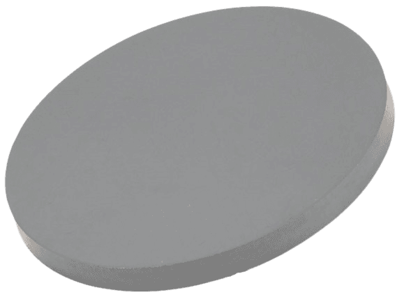
Niobium Telluride (NbTe₂) Sputtering Target is a layered transition metal dichalcogenide (TMD) material valued for its metallic conductivity, low-dimensional structure, and complex electronic behavior. NbTe₂ thin films are actively studied for superconductivity-related phenomena, charge density wave (CDW) characteristics, and advanced electronic devices. As a sputtering target, NbTe₂ enables controlled deposition of uniform telluride thin films for next-generation quantum and optoelectronic research.
Detailed Description
Our NbTe₂ Sputtering Targets are synthesized from high-purity niobium and tellurium sources with strict stoichiometric control to preserve the Nb:Te ratio. Accurate composition is essential, as small deviations can significantly affect electrical conductivity, lattice structure, and phase stability of the deposited film.
The targets are consolidated through carefully optimized sintering or hot-pressing processes to achieve high density and homogeneous microstructure. A dense target body minimizes particle generation and improves plasma stability during sputtering. Due to its semimetallic or metallic conductivity, NbTe₂ is typically compatible with DC sputtering systems, although RF sputtering can also be applied depending on system configuration and film requirements.
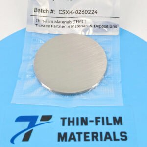
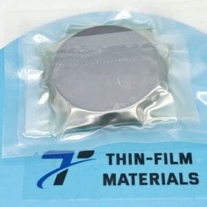
Planar round, rectangular, and custom geometries are available, with optional bonding to copper backing plates for enhanced thermal dissipation in higher-power deposition systems.
Applications
Niobium Telluride Sputtering Targets are widely used in:
Two-dimensional (2D) material thin films
Superconductivity and quantum materials research
Charge density wave (CDW) studies
Metallic and semimetallic thin films
Advanced optoelectronic and electronic devices
Academic and industrial R&D in TMD materials
Technical Parameters
| Parameter | Typical Value / Range | Importance |
|---|---|---|
| Chemical Composition | NbTe₂ | Determines electronic and structural properties |
| Purity | 99.9% – 99.99% | Reduces impurity-related electronic defects |
| Diameter | 25 – 200 mm (custom available) | Compatible with sputtering systems |
| Thickness | 3 – 6 mm | Influences target lifetime |
| Density | ≥ 95% theoretical | Improves plasma stability |
| Sputtering Mode | DC / RF sputtering | Suitable for conductive chalcogenides |
| Bonding | Unbonded / Cu backing (optional) | Enhances thermal management |
Comparison with Related Telluride Materials
| Material | Key Advantage | Typical Application |
|---|---|---|
| NbTe₂ | Layered metallic structure | Quantum & CDW research |
| NbSe₂ | Superconducting behavior | 2D materials research |
| MoTe₂ | Phase-change characteristics | Electronics & photonics |
| WTe₂ | Topological properties | Advanced quantum devices |
FAQ
| Question | Answer |
|---|---|
| Is DC sputtering suitable for NbTe₂? | Yes, NbTe₂ is typically conductive and compatible with DC sputtering. |
| Can the target size be customized? | Yes, diameter, thickness, and bonding options can be tailored. |
| How is stoichiometry maintained during deposition? | Controlled target composition and optimized sputtering parameters ensure stable film chemistry. |
| How is the target packaged? | Vacuum-sealed with protective foam and export-grade cartons or crates. |
Packaging
Our Niobium Telluride Sputtering Targets are meticulously labeled and vacuum-sealed to prevent oxidation and contamination. Protective export-grade packaging ensures safe transportation and storage stability.
Conclusion
Niobium Telluride (NbTe₂) Sputtering Target provides a reliable platform for depositing high-quality layered telluride thin films with unique electronic and structural properties. With precise stoichiometric control, high density, and customizable configurations, it is well suited for advanced quantum materials research and next-generation electronic applications.
For detailed specifications and a quotation, please contact us at sales@thinfilmmaterials.com.

Reviews
There are no reviews yet.