
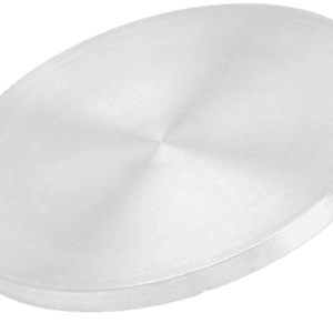
Copper (II) Telluride Sputtering Target
Introduction
The Copper (II) Telluride (CuTe) Sputtering Target is a compound material designed for advanced thin film deposition. With its combination of copper’s electrical conductivity and tellurium’s semiconducting characteristics, it is an important material in optoelectronics, photovoltaics, and semiconductor research. This target enables the production of uniform films with controlled composition, making it highly valuable in both academic research and industrial applications.
Detailed Description
Copper (II) Telluride sputtering targets are produced from high-purity CuTe powders through techniques such as hot pressing, sintering, or vacuum melting. The resulting targets offer:
High Purity (≥99.9%): Ensures minimal contamination for precise thin films.
Stable Phase Composition: Maintains chemical integrity under sputtering conditions.
Uniform Density: Enhances deposition consistency and prolongs target life.
Custom Sizes: Available in diameters ranging from 25 mm to 300 mm, with thicknesses from 3 mm to 6 mm.
Bonding Options: Indium, copper, or elastomer backing plates for thermal management and mechanical stability.
Applications
Copper (II) Telluride sputtering targets are used in multiple cutting-edge fields:
Photovoltaics: For thin film solar cells, particularly in CdTe and related systems.
Optoelectronics: In photodetectors, sensors, and infrared devices.
Semiconductors: Functional layers in microelectronic and thermoelectric devices.
Research & Development: For studying Cu-Te compound films in energy and electronics applications.
Technical Parameters
| Parameter | Typical Value / Range | Importance |
|---|---|---|
| Purity | 99.9% – 99.99% | Reduces contamination, improves film quality |
| Diameter | 25 – 300 mm (custom) | Fits a wide range of sputtering systems |
| Thickness | 3 – 6 mm | Balances sputtering rate and durability |
| Density | ~6.27 g/cm³ | Affects sputtering efficiency |
| Bonding | Indium, Copper, Elastomer | Improves heat dissipation & stability |
Comparison with Related Materials
| Material | Key Advantage | Typical Application |
|---|---|---|
| Copper (II) Telluride (CuTe) | Good balance of conductivity & semiconducting properties | Solar cells, sensors |
| Cadmium Telluride (CdTe) | High absorption coefficient | Thin film photovoltaics |
| Zinc Telluride (ZnTe) | Wide bandgap semiconductor | Optoelectronics, LEDs |
FAQ
| Question | Answer |
|---|---|
| Can Copper (II) Telluride targets be customized? | Yes, dimensions, bonding, and purity levels can be tailored. |
| How are CuTe targets packaged? | They are vacuum-sealed, cushioned with protective foam, and packed in export-safe cartons or crates. |
| What industries use CuTe targets? | Photovoltaics, semiconductors, optoelectronics, and academic R&D. |
| Is backing available for large targets? | Yes, indium, copper, or elastomer backing is available for stability. |
Packaging
Every Copper (II) Telluride sputtering target is carefully vacuum-sealed and cushioned to prevent oxidation or mechanical damage. Clear labeling ensures full traceability, and all shipments are packed in protective cartons or wooden crates for safe global transport.
Conclusion
The Copper (II) Telluride Sputtering Target is a highly reliable compound material for producing advanced thin films in photovoltaics, optoelectronics, and semiconductor applications. With customizable purity, dimensions, and bonding options, it is a trusted choice for both research institutions and industrial manufacturing.
For detailed specifications and a quotation, please contact us at [sales@thinfilmmaterials.com].

Reviews
There are no reviews yet.