 MSDS File
Introduction
Lead Lanthanum Zirconium Titanate (PLZT, Pb₁₋ₓLaₓ(ZrᵧTi₁₋ᵧ)₁₋₀.₂₅ₓO₃) Evaporation Materials are advanced ferroelectric ceramic materials widely used in thin film deposition for electro-optic, piezoelectric, and memory device applications. By incorporating lanthanum into the classic PZT lattice, PLZT exhibits enhanced optical transparency, improved dielectric properties, and modified ferroelectric behavior.
PLZT evaporation materials are specifically engineered for physical vapor deposition (PVD) processes, enabling the fabrication of high-quality ferroelectric and electro-optic thin films in research and industrial environments.
Detailed Description
PLZT is a perovskite-structured complex oxide derived from Lead Zirconium Titanate (PZT), where La³⁺ partially substitutes Pb²⁺. This substitution introduces charge compensation and modifies domain dynamics, dielectric constant, and optical transmission properties.
The compositional flexibility of PLZT allows tuning of two critical parameters:
Lanthanum content (x) – Influences transparency, dielectric response, and domain structure
Zr/Ti ratio (y) – Controls phase structure (tetragonal/rhombohedral) and ferroelectric behavior
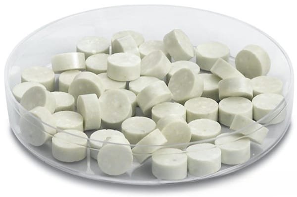
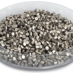
PLZT evaporation materials are typically supplied as:
Sintered ceramic pellets
Granules or pieces for resistive or electron beam evaporation
Custom-shaped evaporation feedstock
To compensate for potential lead volatility during evaporation, compositions are carefully optimized to maintain stoichiometry in deposited films. High-density ceramic processing ensures compositional uniformity and stable evaporation characteristics.
Key performance attributes include:
High dielectric permittivity
Strong electro-optic response
Ferroelectric switching capability
Tunable optical transparency
Stable perovskite phase structure
These characteristics make PLZT an important material for integrated photonics and microelectronic device fabrication.
Applications
Lead Lanthanum Zirconium Titanate (PLZT) Evaporation Materials are widely used in:
Electro-optic modulators
Ferroelectric thin film capacitors
Non-volatile FeRAM devices
Infrared detectors
Transparent ferroelectric devices
Optical shutters and waveguides
MEMS actuators and sensors
Integrated photonic components
PLZT thin films are particularly valuable where both electrical polarization control and optical transparency are required.
Technical Parameters
| Parameter | Typical Value / Range | Importance |
|---|---|---|
| Chemical Formula | Pb₁₋ₓLaₓ(ZrᵧTi₁₋ᵧ)₁₋₀.₂₅ₓO₃ | Defines ferroelectric properties |
| La Content (x) | 0.02 – 0.12 (customizable) | Tunes dielectric & optical response |
| Zr/Ti Ratio (y) | 0.40 – 0.70 (customizable) | Controls phase & polarization |
| Purity | 99.9% – 99.99% (metal basis) | Ensures film uniformity |
| Form | Pellets / Granules / Pieces | Compatible with evaporation systems |
| Density | ≥ 95% theoretical density | Stable evaporation behavior |
| Evaporation Method | E-beam / Resistive | Deposition flexibility |
Comparison with Related Materials
| Material | Key Advantage | Typical Application |
|---|---|---|
| PLZT | Optical transparency + ferroelectricity | Electro-optic devices |
| PZT | Strong piezoelectric response | Actuators & sensors |
| BaTiO₃ | Lead-free dielectric material | Capacitors |
| LiNbO₃ | High electro-optic coefficient | Photonic modulators |
Compared with conventional PZT, PLZT offers improved optical transmission and modified dielectric properties, making it more suitable for optoelectronic and integrated photonic systems.
FAQ
| Question | Answer |
|---|---|
| Can composition be customized? | Yes, both La content and Zr/Ti ratio can be tailored according to application requirements. |
| Is lead volatility considered during evaporation? | Yes, compositions are optimized to compensate for potential lead loss during deposition. |
| What evaporation methods are supported? | Suitable for electron beam and resistive heating evaporation. |
| Can you provide small research quantities? | Yes, flexible quantities are available for R&D applications. |
| How is the material packaged? | Vacuum-sealed packaging with protective cushioning ensures safe transport. |
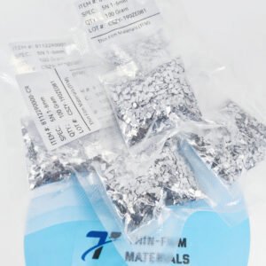
Packaging
Our Lead Lanthanum Zirconium Titanate (PLZT) Evaporation Materials are meticulously tagged and labeled externally to ensure efficient identification and maintain high standards of quality control. We take great care to prevent any potential damage during storage and transportation, ensuring the materials arrive in perfect condition.
Conclusion
Lead Lanthanum Zirconium Titanate (PLZT) Evaporation Materials provide a versatile and tunable solution for depositing high-performance ferroelectric and electro-optic thin films. With adjustable composition, stable perovskite structure, and compatibility with standard PVD processes, PLZT supports advanced device fabrication in photonics, memory technologies, and functional oxide electronics.
For detailed specifications and a quotation, please contact us at sales@thinfilmmaterials.com.

Reviews
There are no reviews yet.