 MSDS File
Introduction
Silicon Carbide (SiC) is a wide-bandgap compound semiconductor recognized for its exceptional thermal stability, high hardness, and chemical inertness. As an evaporation material, SiC is increasingly used in advanced thin film technologies where durability, high-temperature performance, and controlled electrical properties are required. It plays an important role in semiconductor processing, optical coatings, and protective film deposition.
Detailed Description
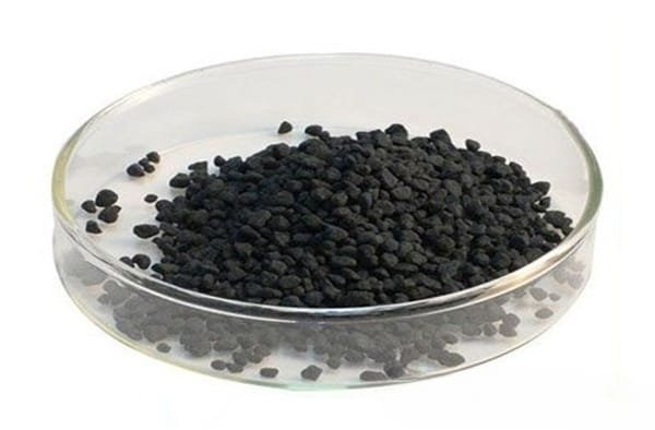
Silicon Carbide Evaporation Materials are produced through high-temperature synthesis of silicon and carbon, followed by crushing, classification, and densification processes. Depending on the application, SiC is supplied in the form of granules, pellets, or custom-shaped pieces suitable for thermal evaporation or electron beam evaporation systems.
SiC has a very high sublimation temperature (above ~2700°C), which makes it particularly suitable for high-energy deposition processes such as electron beam evaporation. Its strong covalent bonding results in excellent mechanical strength and resistance to chemical attack, enabling the formation of stable, wear-resistant thin films.
The stoichiometric balance between silicon and carbon is critical for achieving consistent evaporation behavior and film properties. High-purity SiC materials minimize contamination and ensure uniform film composition, which is especially important in semiconductor and optical applications. Additionally, SiC films are valued for their hardness, thermal conductivity, and resistance to oxidation in harsh environments.
Due to its semiconducting nature and wide bandgap, SiC is also used in applications requiring high-temperature electronics and dielectric layers with specific electrical characteristics.
Applications
Silicon Carbide Evaporation Materials are widely used in:
- Semiconductor thin films and high-temperature electronic devices
- Protective coatings for wear and corrosion resistance
- Optical coatings, including anti-reflective and infrared applications
- Hard coatings for mechanical components and tooling
- Thin film layers in energy and power electronics devices
- Research and development of advanced ceramic and composite films
Technical Parameters
| Parameter | Typical Value / Range | Importance |
|---|---|---|
| Purity | 99.5% – 99.99% | Ensures film quality and minimizes contamination |
| Form | Granules / Pellets / Custom | Compatible with evaporation systems |
| Density | ≥ 90% theoretical | Improves evaporation stability |
| Sublimation Temp | > 2700°C | Suitable for high-temperature deposition |
| Particle Size | 1 – 6 mm (typical) | Affects evaporation rate and uniformity |
| Crystal Structure | α-SiC / β-SiC | Influences film properties |
Comparison with Related Materials
| Material | Key Advantage | Typical Application |
|---|---|---|
| Silicon Carbide (SiC) | High thermal conductivity, extreme hardness | High-temp electronics, protective coatings |
| Silicon (Si) | Easier deposition, lower cost | Semiconductor devices |
| Silicon Nitride (Si₃N₄) | Excellent insulation properties | Dielectric layers, protective films |
FAQ
| Question | Answer |
|---|---|
| Can SiC evaporation materials be customized? | Yes, size, shape, and purity can be tailored to specific evaporation equipment. |
| What deposition method is recommended for SiC? | Electron beam evaporation is commonly used due to the high sublimation temperature. |
| Is SiC suitable for semiconductor applications? | Yes, especially in high-power and high-temperature electronic devices. |
| How should SiC materials be stored? | Store in a clean, dry environment to avoid contamination. |
| What are the advantages of SiC over pure silicon? | SiC offers higher thermal stability, hardness, and resistance to harsh environments. |
Packaging
Our Silicon Carbide Evaporation Materials are meticulously tagged and labeled externally to ensure efficient identification and maintain high standards of quality control. We take great care to prevent any potential damage during storage and transportation, ensuring the materials arrive in perfect condition.
Conclusion
Silicon Carbide Evaporation Materials provide an excellent solution for demanding thin film applications requiring high thermal stability, mechanical strength, and chemical resistance. With flexible customization options and reliable quality, SiC is an ideal choice for advanced industrial and research applications.
For detailed specifications and a quotation, please contact us at sales@thinfilmmaterials.com.


Reviews
There are no reviews yet.