 MSDS File
Indium(III) Sulfide Evaporation Materials Overview
Indium(III) sulfide (In2S3) is a high-quality sulfide ceramic material used in evaporation processes. Known for its exceptional purity, TFM’s Indium(III) sulfide evaporation material ensures superior performance in film deposition, which is critical for achieving high-quality thin films. TFM’s products are manufactured with up to 99.9995% purity, thanks to rigorous quality assurance measures that uphold product reliability and consistency.
Key Specifications
| Material Type | Indium(III) sulfide |
| Symbol | In2S3 |
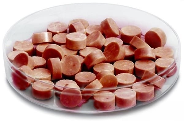
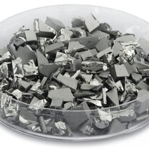
| Appearance/Color | Red Solid |
| Melting Point | 1,050 °C (1,920 °F; 1,320 K) |
| Density | 4.90 g/cm3, solid |
| Purity | 99.9% ~ 99.999% |
| Shape | Powder/ Granule/ Custom-made |
Applications
Indium(III) sulfide evaporation materials are versatile and find applications in various deposition techniques, including:
- Semiconductor Deposition: Essential for creating high-quality semiconductor layers.
- Chemical Vapor Deposition (CVD): Used to deposit thin films for a variety of applications.
- Physical Vapor Deposition (PVD): Ideal for depositing coatings on substrates.
These materials are particularly useful in optics for:
- Wear Protection: Enhancing the durability of optical components.
- Decorative Coatings: Adding aesthetic value to surfaces.
- Displays: Ensuring high performance and quality in display technologies.
Packaging and Handling
TFM ensures that Indium(III) sulfide materials are packaged with care to prevent damage during storage and transportation. Each package is clearly labeled for easy identification and quality control.
Contact Us
TFM is a prominent supplier of high-purity Indium(III) sulfide evaporation materials. We offer a variety of forms, including tablets, granules, rods, and wires, with custom solutions available upon request. Additionally, TFM provides evaporation sources, boats, filaments, crucibles, heaters, and e-beam crucible liners. For current pricing and additional information, please reach out to us with your inquiry.


Reviews
There are no reviews yet.