 MSDS File
Gallium(III) Selenide Evaporation Materials Description
Gallium(III) selenide evaporation material, with the chemical formula Ga₂Se₃, is a specialized selenide ceramic used in high-precision deposition processes. TFM offers gallium(III) selenide with exceptional purity levels up to 99.9995%, ensuring that the films deposited are of the highest quality. This material is critical in various applications where precision and reliability are paramount.
Specifications of Gallium(III) Selenide Evaporation Materials
| Material Type | Gallium(III) Selenide |
| Symbol | Ga2Se3 |
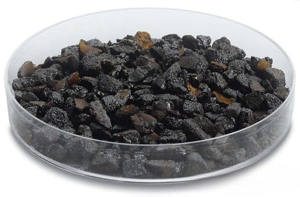
| Appearance/Color | Reddish-black crystals |
| Melting Point | 1,020 °C (1,870 °F; 1,290 K) |
| Density | 4.92 g/cm3 |
| Purity | 99.9% ~ 99.999% |
| Shape | Powder/ Granule/ Custom-made |
Applications of Gallium(III) Selenide Evaporation Materials
Gallium(III) selenide is primarily used in semiconductor deposition techniques, including chemical vapor deposition (CVD) and physical vapor deposition (PVD). It is particularly valuable in optics for applications such as wear-resistant coatings, decorative finishes, and display technologies.
Packaging and Handling
TFM ensures that gallium(III) selenide materials are carefully packaged with clear labeling for easy identification and quality control. The packaging is designed to protect the material from damage during storage and transit.
Contact Information
As a premier supplier of high-purity gallium(III) selenide evaporation materials, TFM provides a range of options including tablets, granules, rods, and wires. Custom shapes and quantities are available upon request. In addition to evaporation materials, TFM offers evaporation sources, boats, filaments, crucibles, heaters, and e-beam crucible liners. For pricing and inquiries, please contact us directly.


Reviews
There are no reviews yet.