Generic selectors
Exact matches only
Search in title
Search in content
Post Type Selectors

VD0849 Lead Selenide Evaporation Materials, PbSe

Catalog No.VD0849
MaterialLead Selenide (PbSe)
Purity99.9% ~ 99.999%
ShapePowder/ Granule/ Custom-made

TFM stands out as a top manufacturer and supplier specializing in high-purity lead selenide evaporation materials, alongside a diverse range of other evaporation materials. We provide these materials in both powder and granule formats, with options for custom formulations available upon request.

Lead Selenide Evaporation Materials Overview

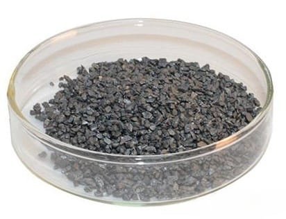
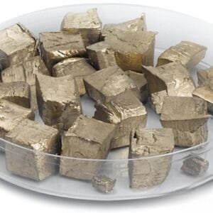
Lead selenide (PbSe) is a high-purity ceramic material used extensively in various deposition techniques. Our lead selenide evaporation materials are crafted to meet the highest standards, with a purity of up to 99.9995%. These materials are crucial for ensuring top-notch quality in deposited films.

Specifications

Material TypeLead Selenide
SymbolPbSe
Appearance/ColorGray solid
Melting Point1,078 °C (1,972 °F; 1,351 K)
Density8.1 g/mL at 25 °C
Purity99.9% ~ 99.999%
ShapePowder/ Granule/ Custom-made

Applications

Our lead selenide evaporation materials are designed for use in a variety of deposition processes, including:

  • Semiconductor Deposition
  • Chemical Vapor Deposition (CVD)
  • Physical Vapor Deposition (PVD)

These materials are predominantly used in optical applications such as wear-resistant coatings, decorative finishes, and display technologies.

Packaging

Each batch of lead selenide evaporation materials is meticulously tagged and labeled to facilitate easy identification and quality assurance. We ensure that all materials are handled with care during storage and transportation to prevent any damage.

Contact Us

As a prominent manufacturer and supplier of high-purity lead selenide evaporation materials, we offer a range of forms including tablets, granules, rods, and wires. Custom shapes and quantities are available upon request. In addition to evaporation materials, we also provide evaporation sources, boats, filaments, crucibles, heaters, and e-beam crucible liners. For pricing information or to inquire about materials not listed, please contact us.

Reviews

There are no reviews yet.

Be the first to review “VD0849 Lead Selenide Evaporation Materials, PbSe”

Your email address will not be published. Required fields are marked *

FAQ

  • They are high‐purity substances (e.g. metals, alloys, or compounds) used in thermal or electron‐beam evaporation processes to form thin films on substrates.

  • Typically, they’re processed into a form (often ingots, pellets, or wires) that can be efficiently vaporized. Preparation emphasizes high purity and controlled composition to ensure film quality.

  • Thermal evaporation and electron-beam (e-beam) evaporation are the two main techniques, where material is heated (or bombarded with electrons) until it vaporizes and then condenses on the substrate.

  • Thermal evaporation heats the material directly (often using a resistive heater), while e-beam evaporation uses a focused electron beam to locally heat and vaporize the source material—each method offering different control and energy efficiency.

  • Key parameters include source temperature, vacuum level, deposition rate, substrate temperature, and the distance between the source and the substrate. These factors influence film uniformity, adhesion, and microstructure.

  • Evaporation generally produces high-purity films with excellent control over thickness, and it is especially suitable for materials with relatively low melting points or high vapor pressures.

  • Challenges include issues with step coverage (due to line-of-sight deposition), shadowing effects on complex topographies, and possible re-evaporation of material from the substrate if temperature isn’t properly controlled.

  • Common evaporation materials include noble metals (e.g., gold, silver), semiconductors (e.g., silicon, germanium), metal oxides, and organic compounds—each chosen for its specific optical, electrical, or mechanical properties.

  • Selection depends on desired film properties (conductivity, optical transparency, adhesion), compatibility with the evaporation process, and the final device application (semiconductor, optical coating, etc.).

  • Optimizing substrate temperature, deposition rate, and chamber vacuum are critical for ensuring that the film adheres well and forms the intended microstructure without defects.

  • Troubleshooting may involve checking the source material’s purity, ensuring stable source temperature, verifying the vacuum level, adjusting the substrate’s position or temperature, and monitoring deposition rate fluctuations.

While evaporation tends to yield very high purity films with excellent thickness control, it is limited by its line-of-sight nature. In contrast, sputtering can deposit films more uniformly on complex surfaces and is more versatile for a broader range of materials.


Shopping Cart
Scroll to Top