 MSDS File
Introduction
Tungsten Diselenide (WSe₂) Evaporation Materials are advanced transition metal dichalcogenide (TMD) sources used for depositing high-quality semiconducting thin films in physical vapor deposition (PVD) processes. With a tunable bandgap, strong spin–orbit coupling, and excellent layered crystallinity, WSe₂ has become a key material for next-generation electronics, optoelectronics, and 2D material research. Evaporation-grade WSe₂ enables controlled film growth for both exploratory R&D and device prototyping.
Detailed Description
WSe₂ evaporation materials are synthesized from high-purity tungsten and selenium precursors with precise stoichiometric control to ensure a stable W:Se ratio. The material is processed into evaporation-friendly forms through controlled synthesis and consolidation steps, minimizing residual impurities and volatile contamination.
As a layered van der Waals material, WSe₂ can be deposited via thermal evaporation or electron-beam evaporation under high vacuum. Proper source geometry and evaporation rate control are essential to maintain compositional fidelity and achieve smooth, continuous films. Deposited WSe₂ films can range from ultrathin layers suitable for 2D electronics to thicker films for optoelectronic and sensing applications.
Compared with oxide or metallic evaporation materials, WSe₂ offers intrinsic semiconducting behavior without the need for post-deposition oxidation or sulfurization/selenization steps, simplifying process integration for TMD-based devices.
Applications
Tungsten Diselenide evaporation materials are widely used in:
2D electronics: Channel layers for field-effect transistors (FETs)
Optoelectronics: Photodetectors, light-emitting and light-absorbing devices
Spintronics & valleytronics: Materials research leveraging strong spin–orbit coupling
Flexible electronics: Thin, mechanically compliant semiconductor films
Heterostructures: van der Waals stacks with graphene and other TMDs
Academic & industrial R&D: Fundamental studies of layered semiconductors
Technical Parameters
| Parameter | Typical Value / Range | Importance |
|---|---|---|
| Chemical Composition | WSe₂ (Tungsten Diselenide) | Defines electronic and optical properties |
| Purity | 99.9% – 99.99% | Reduces defect density in films |
| Stoichiometry | W:Se ≈ 1:2 | Ensures semiconducting behavior |
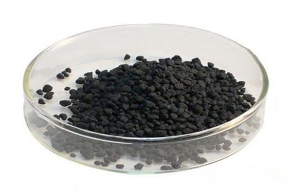
| Form | Pieces, pellets, granules | Compatible with evaporation sources |
| Evaporation Method | Thermal / E-beam | Flexible PVD integration |
| Crystal Nature | Layered (van der Waals) | Enables 2D thin-film applications |
Comparison with Related TMD Materials
| Material | Key Advantage | Typical Application |
|---|---|---|
| WSe₂ | Tunable bandgap, ambipolar transport | 2D electronics & optoelectronics |
| MoS₂ | Mature process ecosystem | FETs and sensors |
| WS₂ | Strong light–matter interaction | Photonics |
| MoSe₂ | Narrower bandgap | Infrared optoelectronics |
FAQ
| Question | Answer |
|---|---|
| Can WSe₂ evaporation materials be customized? | Yes, purity, form, and batch size can be tailored. |
| Which evaporation method is recommended? | Both thermal and electron-beam evaporation are used, depending on system design. |
| Is post-annealing required? | Optional annealing can improve crystallinity for certain applications. |
| How are the materials packaged? | Vacuum-sealed with moisture- and contamination-resistant protection. |
Packaging
Our Tungsten Diselenide Evaporation Materials (WSe₂) are carefully labeled for traceability and packaged using vacuum sealing with reinforced cushioning. This packaging approach protects against moisture uptake, selenium loss, and mechanical damage during storage and transportation.
Conclusion
Tungsten Diselenide Evaporation Materials (WSe₂) provide a reliable pathway to deposit high-quality TMD thin films with well-defined semiconducting properties. With controlled stoichiometry, flexible evaporation formats, and consistent material quality, WSe₂ is an essential evaporation source for advanced 2D electronics and optoelectronic research.
For detailed specifications and a quotation, please contact us at sales@thinfilmmaterials.com.


Reviews
There are no reviews yet.