 MSDS File
Molybdenum Ditelluride Evaporation Materials Overview
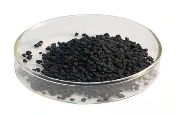
Molybdenum ditelluride (MoTe₂) is a high-purity telluride ceramic used as an evaporation material in various deposition processes. At TFM, we specialize in producing MoTe₂ with exceptional purity levels, reaching up to 99.9995%. Our rigorous quality control ensures that our products deliver reliable performance in film deposition.
Product Specifications
| Material Type | Molybdenum Ditelluride |
| Symbol | MoTe2 |
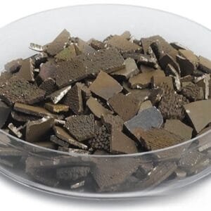
| Appearance/Color | Black/lead-gray solid |
| Melting Point | Decomposes |
| Density | 7.7 g/cm3 |
| Purity | 99.9% ~ 99.999% |
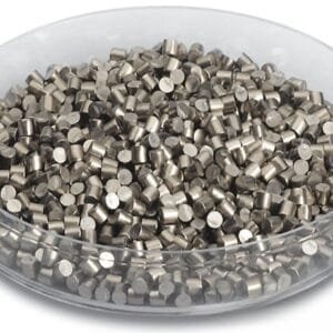
| Shape | Powder/ Granule/ Custom-made |
Applications
Molybdenum ditelluride is utilized in several key areas, including:
- Semiconductor Deposition: Essential for creating thin films in semiconductor devices.
- Chemical Vapor Deposition (CVD): Used to produce high-quality thin films and coatings.
- Physical Vapor Deposition (PVD): Ideal for depositing films in various electronic and optical applications.
- Optics: Employed for wear protection, decorative coatings, and display technologies.
Packaging Information
Our MoTe₂ evaporation materials are meticulously packaged in plastic vacuum bags to ensure they remain undamaged during storage and transit. Each package includes a Certificate of Analysis (COA) to verify the material’s quality and specifications.
Contact Us
At TFM, we pride ourselves on delivering high-quality molybdenum ditelluride evaporation materials tailored for advanced applications in semiconductors, CVD, PVD, and optical fields. Our experienced engineering, manufacturing, and analytical teams work together to produce top-tier materials. For inquiries or to request a quote, please contact us today.

Reviews
There are no reviews yet.