Ceramic Substrates


Ceramic Substrates for Thin Film, Microelectronic, and High-Temperature Applications
ThinFilmMaterials offers a wide range of high-performance Ceramic Substrates engineered for use in vacuum deposition, semiconductor processing, electronic packaging, and optical applications. These substrates provide excellent electrical insulation, thermal stability, and dimensional precision under extreme conditions.
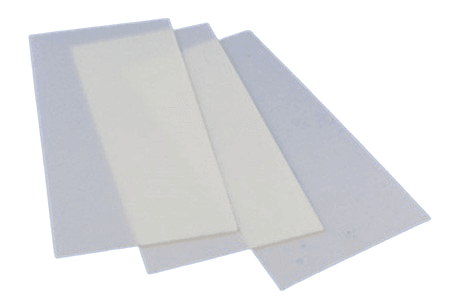
Our Ceramic Substrates are available in a variety of materials, including alumina (Al₂O₃), aluminum nitride (AlN), zirconia (ZrO₂), silicon nitride (Si₃N₄), and quartz. Each material is selected based on its dielectric properties, thermal conductivity, and compatibility with specific deposition or circuit integration processes.
Key Features of Ceramic Substrates:
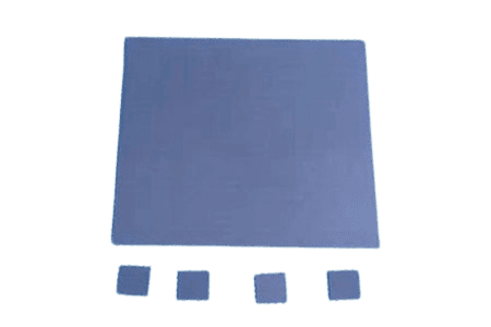
Materials: Alumina, Aluminum Nitride, Zirconia, Quartz, Silicon Nitride
Surface finish: Lapped, polished, or as-fired
Thicknesses: From 0.25 mm to 5 mm (custom options available)
Tolerance: Tight dimensional control for mask alignment and precision patterning
Properties: High thermal resistance, excellent dielectric strength, corrosion resistance
Applications:
Ceramic Substrates are widely used in:
Sputtering and evaporation deposition platforms
Microelectronics and hybrid circuit packaging
Laser diode mounting and RF components
Insulating spacers in vacuum or high-voltage systems
Optical windows and sensors in harsh environments
At ThinFilmMaterials, we provide Ceramic Substrates in standard wafer sizes (1″–6″) as well as custom-machined dimensions. Substrates can be supplied polished on one or both sides, with optional metallization or laser patterning services upon request.